
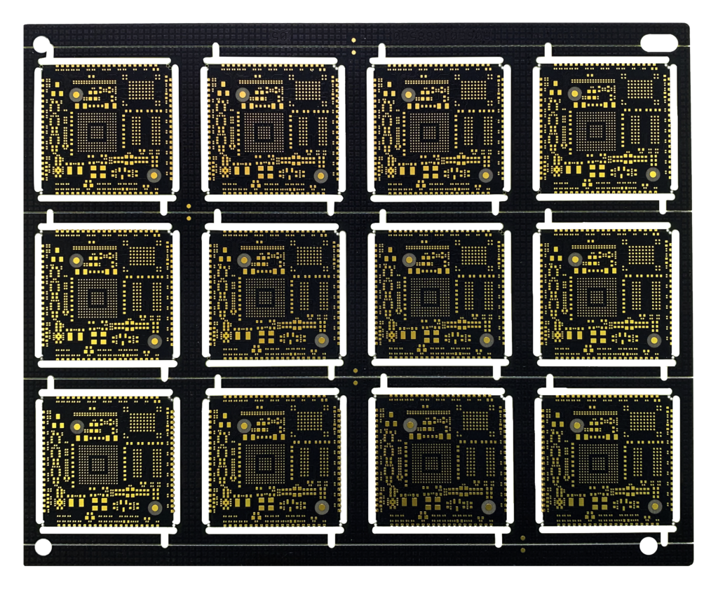
What is a Multi-layer PCB?
Multi-layer PCB is also one of our circuit designs. It is more like a combination of single-layer and double-layer PCB. We can see it in some application circuit boards that require extremely high precision and conditions. Therefore, we will provide relevant information, advantages, and characteristics below.
Understand the structure of multi-layer PCB
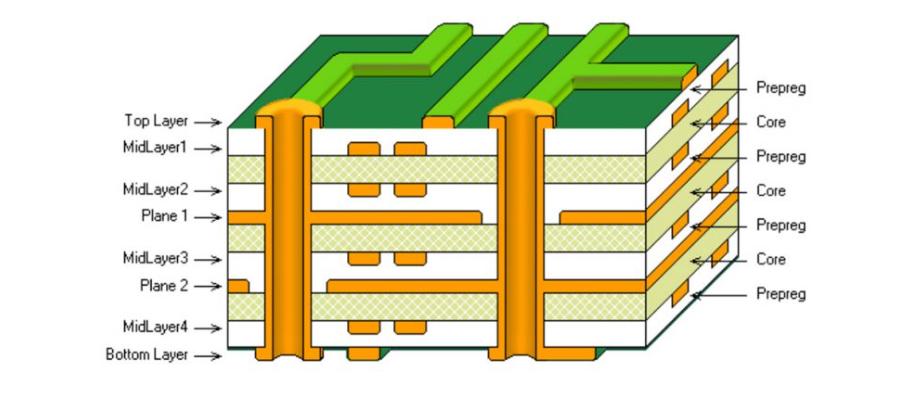
Multi-layer PCBs have complex structures. Unlike single- or double-layer PCBs, multilayer PCBs contain multiple layers of conductive traces and insulating materials, providing a three-dimensional platform for intricate circuit designs.
Their core structure consists of alternating copper and insulating substrate layers, often called core and prepreg layers. The manufacturing process involves laminating these layers under controlled heat and pressure to form a robust and integrated structure. The interconnect board etches the copper layer into the circuit pattern of the electronic components.
Internal layers sandwiched between core layers form internal circuits. Designers strategically place signal, power, and ground planes on these layers to enhance signal integrity and reduce electromagnetic interference. Connecting these inner layers are vias, small holes filled with conductive material. Vias run throughout the board, while blind and buried vias connect only specific layers. Multilayer PCBs have additional copper traces on the outer layers and may include surface mount components. Solder mask covers the conductive traces, protecting them from accidental short circuits.
Functionality and Versatility: How Multilayer PCBs Improve Performance
Multi-layer PCBs are more complex than single-layer or double-layer PCBs. We can improve multi-layer PCB performance from the following key factors.
Enhanced signal integrity: Multi-layer PCBs can use internal ground and power planes distributed across layers. This architecture minimizes signal interference, reduces crosstalk between traces, and improves signal integrity.
Optimized thermal management: The PCB’s multiple layers allow for efficient heat dissipation. Electronic components can disperse and conduct heat to critical areas, preventing overheating and ensuring equipment reliability and longevity.
Reduce electromagnetic interference (EMI): Internal ground and power planes can act as shields between signal layers, reducing potential electromagnetic interference. This feature is critical for applications that maintain clean and stable signals, such as communications systems and high-frequency circuits.
Improved Power Distribution: Adding internal power planes improves power distribution efficiency on the PCB. This primarily benefits devices with multiple power domains, ensuring stable and reliable power delivery to all components.
Multi-layer PCB Manufacturing process
Manufacturing a multi-layer printed circuit board (PCB) requires precise steps to create complex electronic circuits with enhanced functionality. Below are the process steps we enumerate for multi-layer PCB manufacturing.
Design and CAD layout:
Engineers create detailed designs using CAD software, including layer stacking, component placement, and trace routing.
material selection:
Select high-quality materials, including copper-clad laminates and prepreg layers, with specific dielectric properties, thermal characteristics, and compatibility with the intended application.
Layer stacking and lamination:
Their core layers are made of fiberglass-reinforced epoxy resin, combined with prepreg layers to form a layup. The stack is subjected to heat and pressure in a laminator, creating a solid structure.
Drilling:
Drilling small holes or vias through the layer stack facilitates interlayer connections. Vias can be through holes, blind holes, or buried holes, depending on the customer’s design requirements.
Copper plating:
To enhance conductivity and ensure electrical continuity between layers, plate the drilled holes with copper.
PCB layer design
Inner layer imaging:
Photolithography is used to transfer the PCB design onto the internal copper layer. A layer of photoresist is applied and exposed to UV light through a mask, revealing the circuit traces. The excess copper is then chemically etched to remove it.
Inner layer inspection:
Rigorous quality inspections, including visual checks and automated optical inspection (AOI), are required to verify the accuracy and integrity of the inner circuitry.
Pre-glued:
Adding prepreg layers and pre-bonding, the layup occurs before it enters the laminator again. This step ensures a strong and even bond between the layers.
Outer layer imaging:
Similar to how designers image the inner layers, they photoetch the outer copper layer to define the circuit pattern. Chemical etching removes excess copper and shapes the external traces.
Solder mask application:
Apply a solder mask to protect exposed copper surfaces from oxidation and accidental electrical contact during assembly.
Surface finish:
Surface-treat exposed copper surfaces to enhance solderability and provide corrosion resistance. Common surface treatments include HASL, ENIG, etc.
Final test:
The finished multi-layer PCB, including electrical testing and visual inspection, is thoroughly tested to ensure compliance with standards.
Component assembly:
To complete the manufacturing process, assemble components with the manufactured PCB.
Coping with design complexity
The design and manufacturing of multilayer printed circuit boards (PCBs) present a unique set of challenges, particularly in managing the complexity that arises from increased layer counts and advanced functionality, mainly on the issue of signal integrity, which becomes critical with multiple layers due to the possibility of crosstalk, impedance mismatch, and signal attenuation. So, we can combine controlled impedance design techniques, electromagnetic simulation tools, and differential pair routing strategies to help mitigate signal integrity issues and ensure reliable, high-performance circuits.
The second is that increasing the number of layers will cause heat concentration, affecting the overall thermal performance of the PCB and potentially affecting component reliability. Our advanced thermal analysis tools help optimize copper distribution, integrate heat dissipation structures, and select appropriate materials to enhance thermal conductivity to ensure effective thermal management.
Final
We have learned about the manufacturing process and design characteristics of multi-layer PCBs. Their multiple layers make them suitable for complex automotive control systems, consumer electronics, and industrial control systems to achieve specific functions.