
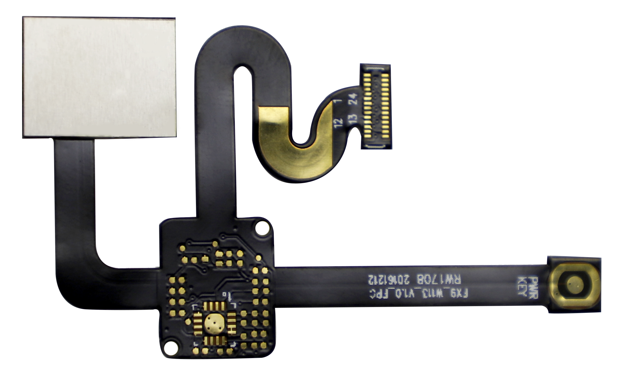
Technical information guide on 2 layer FR4 PCB
Today, we will introduce a kind of PCB, which is also one of the types our consumers often buy. Therefore, we want to let more professional technicians and novices know more about 2 layer FR4 PCB so that we will introduce their relevant information individually in this guide. Let everyone know better!
Understanding 2 Layer FR4 PCB Structure
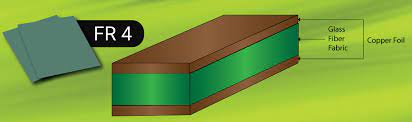
The core of a 2 layer FR4 PCB consists of a substrate made of type 4 flame retardant (FR4) material (glass-reinforced epoxy laminate). The “2-layer” designation means that the PCB comprises two copper layers (one on top and one on the bottom), with the top or signal layer acting as the leading platform for routing traces and placing components. Below the top layer is the ground plane, forming the second layer of the PCB. This layer serves multiple purposes, serving as a signal return path, providing a reference voltage, and mitigating electromagnetic interference. The dielectric material between the top layer and the ground plane is typically FR4, chosen for its electrical insulation properties and mechanical stability.
Their via structure is conducive to the electrical connection between the top and ground layers, thereby completing the circuit path. You can add a silkscreen layer to increase structural stability and mechanical strength to provide component marking. The silkscreen layer helps identify components and ensures accurate placement during manufacturing.
Advantages of FR4 material
From the above paragraphs, we can know that FR4 is a flame-retardant epoxy laminate with fiberglass reinforcements, and its advantages are as follows:
Electrical Insulation: The main advantage of FR4 is its excellent electrical insulation properties. The material effectively prevents unwanted current flow between traces and layers, ensuring circuit integrity and preventing short circuits.
Dielectric Strength: FR4 has high dielectric strength, allowing it to withstand high voltages without breakdown. This property is critical for applications that require insulation between conductive components to prevent electrical discharges.
Thermal Stability: It also has excellent thermal stability, allowing it to withstand a wide temperature range without affecting its structural integrity.
Mechanical Strength: FR4’s woven glass reinforcement helps improve the material’s durability and reliability. This robustness is critical for PCBs subject to mechanical stress during handling, assembly, and use conditions.
Flame retardant: FR4, as a flame retardant material, can significantly reduce the risk of fire spread.
Dimensional stability: FR4 can maintain dimensional stability under different environmental conditions, minimizing changes in size and shape.
Ease of Fabrication: FR4 is well suited for standard PCB manufacturing processes, including drilling, etching, and soldering. Its compatibility with traditional manufacturing technologies simplifies production, reducing production time and costs.
Application of 2 layer FR4 PCB
2 layer FR4 PCB covers a variety of applications due to its material properties and versatility:
Consumer Electronics: 2 layer FR4 PCBs are commonly used in smartphones, tablets, and wearables.
Industrial control system: A 2 layer FR4 PCB is used in the control system. Its rugged construction and stable electrical performance ensure consistent performance in industrial environments.
Automotive Electronics: The automotive industry benefits from 2 layer FR4 PCBs in applications such as engine control units, infotainment systems, and sensors. Their ability to withstand varying temperatures and mechanical stresses meets automotive requirements.
Telecommunications: In the telecommunications sector, networks, base stations, and communication equipment use 2-layer FR4 PCBs. Their cost-effectiveness and consistent electrical performance make them suitable for high-volume production.
Power Supply: Power supply units in industrial and consumer applications typically use 2-layer FR4 PCBs. They handle moderate power loads well, and route power traces efficiently.
What to pay attention to when designing the layout of a 2 layer FR4 PCB
The form of our 2 layer FR4 PCB also requires careful attention to various factors to ensure optimal functionality, signal integrity, and manufacturability.
Component placement: We need targeted and planned placement of components to minimize trace lengths and reduce signal delays. We must also group members according to function to enhance signal flow and simplify layout.
Signal Integrity: Attention signal integrity by minimizing trace lengths, avoiding sharp corners, and maintaining consistent trace widths.
Ground plane: Make sure a solid and continuous ground plane on the bottom layer is a reference for the signal return path. This minimizes noise and enhances EMC.
Power layer: The designer incorporates a dedicated power layer into the top layer to provide a stable power distribution network. This helps reduce voltage drops and ensures consistent power delivery to components.
Trace routing: Route traces carefully to avoid crosstalk and interference. Use wider traces for power lines and high current paths while using controlled impedance traces for sensitive signals.
Decoupling capacitor: The decoupling capacitor should be placed close to the IC power pin to stabilize power distribution and suppress voltage fluctuations.
Heat dissipation considerations: Heating components must also be planned to achieve efficient heat dissipation.
Vias: Use vias judiciously to connect traces between layers. Ensure proper spacing and placement to avoid signal attenuation and interference. Place vias close to components for efficient routing.
Production process
The 2 layer FR4 PCB production involves multiple stages of transforming the design into a functional and manufacturable board. The following are the production steps:
Design and Layout: The first step is to use PCB design software to create a detailed plan and layout. Engineers define the structure of components, traces, vias, and layers based on electrical performance, signal integrity, and manufacturability.
Gerber file generation: The engineer will generate the file after completing the design. These files include information about copper layers, solder masks, screen printing, and drilling files.
Material selection: FR4 is the base material due to its electrical properties and mechanical stability. Usually, manufacturers laminate a thin foil of copper to the FR4 substrate for the copper layer.
Cutting the substrate: Cut the FR4 material into individual panels or sheets according to the dimensions specified in the design.
Cleaning and Surface Preparation: The substrate undergoes a thorough cleaning process to remove contaminants. Surface preparation involves applying a thin layer of copper to the substrate and laying the foundation for the copper traces.
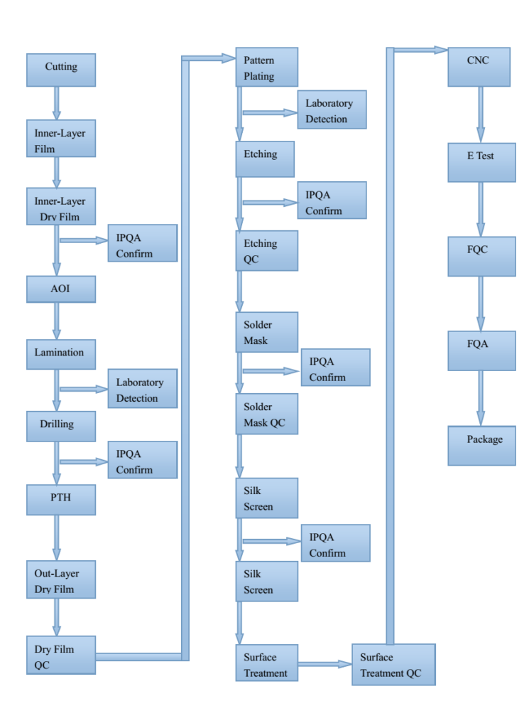
Drilling printing
Printing and Etching the Copper Layer: A photoresist layer is applied to the copper-clad substrate. The Gerber file directs the exposure and development of the photoresist, leaving behind the required copper traces. The etching removes the excess copper, leaving only the intended circuit pattern.
Drilling: Precision drilling creates holes for component mounting and vias.
Through-hole plating: A thin layer of copper is electroplated onto the walls of a drilled hole, creating a conductive path between the layers. This process, called through-hole plating, ensures electrical continuity.
Apply solder mask: Apply it on the copper traces to insulate and protect them. The solder mask also provides a unique color that aids component identification and prevents solder bridges during assembly.
Screen Printing: Information such as component labels, reference designators, and logos are printed onto the surface of a circuit board using a screen printing layer.
Surface Treatment: Surface treatment protects exposed copper and enhances solderability. Common surface treatments include HASL, ENIG, and OSP.
Testing: The production team thoroughly tests every PCB to verify electrical connections, check for shorts, and ensure the board meets design specifications. We usually use automated testing equipment.
Final Inspection and Packaging: The finished printed circuit board undergoes a final inspection to identify any defects or imperfections. Once approved, the production team cuts the circuit boards from the production panels and packages them for shipment or further assembly.
At the end
Through the above technical guide, we want more novices, professionals, and industry stakeholders to know the technical information of 2 layer FR4 PCB. In this way, we can apply it more flexibly in our production and get more related types of PCBs on our official website. Let’s take a look!