Today, we will tell you some relevant knowledge about double layer PCB. From the literal meaning, double layer PCB is distinguished by its double-layer structure. Unlike their single-layer counterparts, this design has two layers of conductive material separated by an insulating layer, making it ideal for complex circuits. As a result, they are suitable for many industries and applications, from consumer electronics to aerospace technology. Let’s take a look at it from our perspective!
Discussing Double Layer PCBs
A double layer PCB is a PCB with conductive layers on both sides of the board. Plated holes interconnect these layers, creating more complex and compact circuit designs. Their structural makeup can help increase circuit complexity, allowing engineers to integrate more components and functions within limited layout space. Generally speaking, double layer PCBs are very suitable for compact and small electronic equipment because they provide more wiring options. Mounting plug-ins on both sides actively reduce the board footprint.

Advantages of Double Layer PCB
Double layer PCBs offer several advantages. First and foremost, they offer greater design flexibility, allowing for a more compact arrangement of components. By utilizing both sides of the circuit board, the layout of traces and features can be optimized for efficient trace routing, thereby reducing the overall footprint of the circuit. Secondly, it also helps improve signal integrity. Placing components on both sides of the board minimizes signal interference and crosstalk. This is critical to maintaining the performance and reliability of electronic circuits, especially in high-frequency applications.
Double layer PCB design principles
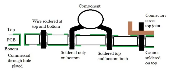
A double layer PCB adds an internal power layer and ground layer. Designers primarily route power and ground networks on the power layer. They have conductive metal on both sides of each substrate layer, and a unique adhesive is used to join the boards together, with insulating material between each panel. However, double-layer wiring is mainly based on the top and bottom layers, supplemented by intermediate wiring layers. Other fundamental aspects include component placement, routing, layer stacking, layout, grounding, power distribution, and more.
Component layout considers the components’ arrangement to ensure efficient signal flow and thermal performance. Some high-speed and sensitive parts can achieve effective heat dissipation through good positioning.
Connecting relevant components through precise wiring design reduces interference and maintains signal integrity. Routing engineers actively route high-speed digital signals through a controlled impedance, ensuring careful matching of differential pairs. Keep signal traces away from noisy components to reduce crosstalk and electromagnetic interference.
PCB layer stacking refers to the multi-layer structure design of a printed circuit board. Usually, a standard multi-layer PCB consists of four main layers: top layer, inner layer, ground layer, and bottom layer. Designers must consider signal integrity, impedance control, power distribution, EMI suppression, and manufacturing feasibility when designing our layer stack.
The specific arrangement and planning of vias via layout design. A conductive path, known as a via, connects different layers of a PCB and establishes connections between the top, bottom, and inner layers. The layout of vias has an essential impact on circuit performance, signal integrity, and manufacturing processes.
Grounding and power distribution are two critical aspects of double-layer PCB design. They have an essential impact on the circuit’s performance, stability, and signal integrity. A grounded double-layer PCB design usually connects a dedicated ground plane layer to the top and bottom layers through vias (Via) to form a low-impedance current return path. Power distribution has dedicated power and ground planes carrying power current and connecting power.
Final summary
We know what double layer PCBs are and how they are designed. Due to their compact design, they are suitable for sensors in industrial automation, electronic systems in automobiles, etc. We hope that through these articles, we can learn more about PCB.