Multi-layer PCB is crucial in modern electronics, allowing for more complex and compact circuit designs. They consist of multiple layers of conductive copper traces and insulating substrate material.
Multilayer board parameters
Number of Layers: Multilayer PCBs can have three or more layers. Layer count is critical and indicates how many individual copper and substrate layers are used in the PCB. Standard multi-tier options include 4, 6, 8 and even higher tiers.
Board Thickness: The overall thickness of a multilayer PCB depends on the number of layers and the thickness of the core and prepreg materials used. Typical thickness range is 0.8 mm to 3.2 mm.
Copper Weight: The inner and outer layers of a multilayer PCB can have different copper weights. Standard copper weights are 1 oz (35μm) for the inner layer and 1 oz or 2 oz for the outer layer.
Materials: Multilayer PCBs use a combination of core and prepreg materials. FR-4 has become a commonly used substrate material due to its good electrical and thermal properties. Materials such as Rogers or Teflon can be used for high frequency applications.
Trace Width and Spacing: The width and spacing of copper traces determine the PCB’s ability to handle high-speed and high-frequency signals. These parameters are critical for impedance control.
Finished Copper Thickness: Final copper thickness is critical to PCB performance and durability. It is determined by the initial copper thickness and the amount of copper remaining after the manufacturing process.
Size: Double-sided PCBs come in a variety of sizes and shapes and can be tailored to the specific requirements of the device in which they are used. Standard sizes (such as 4×6 inches) are typical, but custom sizes are available for unique applications.
Copper Thickness: The thickness of the copper layer on a double-sided PCB is measured in ounces per square foot (oz/ft²). Standard thicknesses include 1 oz and 2 oz, with thicker copper providing better current carrying capabilities.
Hole Size: Double-sided PCBs have holes for component leads or connectors. The accuracy and size of these holes are critical to ensuring proper component alignment and soldering.
Solder mask and silk screen: Solder mask is a protective layer applied to the PCB to prevent solder bridges and corrosion. A silkscreen layer is used for component markings and indicators.
If necessary, you can click to view more of our cases.
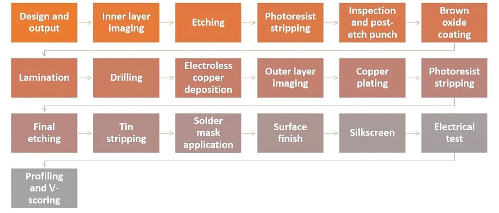
Manufacturing Process of Multi-Layer PCB
Design and Layout: The PCB design process involves creating a circuit layout, specifying layer stack-up, determining trace widths and spacing, and adding necessary components. PCB design software is used for this purpose.
Layer Stacking: A multilayer PCB consists of alternating core material and prepreg layers, with copper foil bonded to each layer. Stacking arrangements are designed to meet electrical and mechanical requirements.
Inner layer processing: A photoresist mask and chemical etching are used to etch the copper layer to create the desired circuit pattern. Then, a thin oxide layer is applied to prevent the copper from oxidizing.
Lamination: The core, prepreg, and copper foil are laminated under heat and pressure to form a single multilayer structure. This is usually done in a hydraulic press.
Drilling: Precision CNC machines drill holes for through-holes and through-hole components. Laser drilling is used to create micro-holes in high-density boards.
Copper plating: Electroplating chemicals add more copper to the inner layer, ensuring the desired copper thickness.
Circuit Imaging: This involves transferring the PCB design to the outer layers using a photoresist and UV exposure process. Chemical etching is used to remove unwanted copper.
Solder mask and screen printing: A solder mask insulates and protects copper traces. Silkscreen layers add component labels and reference indicators.
Surface treatment: Surface treatment prevents copper from oxidizing and facilitates soldering. Standard surface treatments include HASL (Hot Air Solder Leveling), ENIG (Electroless Nickel Immersion Gold) and OSP (Organic Solderability Preservative).
Testing: The PCB undergoes various tests, including electrical testing, to ensure it meets design specifications.
Assembly: Use a placement machine to assemble the components onto the PCB, then reflow the board to connect the pieces.
Final Inspection: The final inspection checks for defects and verifies the proper functionality of the assembled PCB.
Advantages of Multi-layer PCB
✔ Telecommunications Gnetworks, satellite communication, and RF devices.
✔ Consumer Electronics: Smartphones, tablets, and smart wearables.
✔ Medical Devices: MRI scanners, diagnostic equipment, and implants.
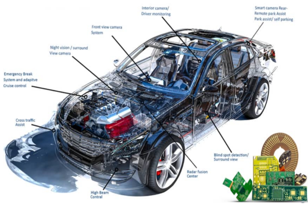
✔ Automotive Electronics: ADAS, EV battery management, and infotainment systems.
✔ Aerospace & Defense: Radar, avionics, and military-grade electronics.
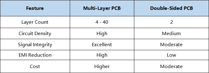
Multi-layer PCB VS. Double-Sided PCB
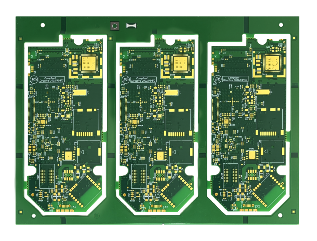
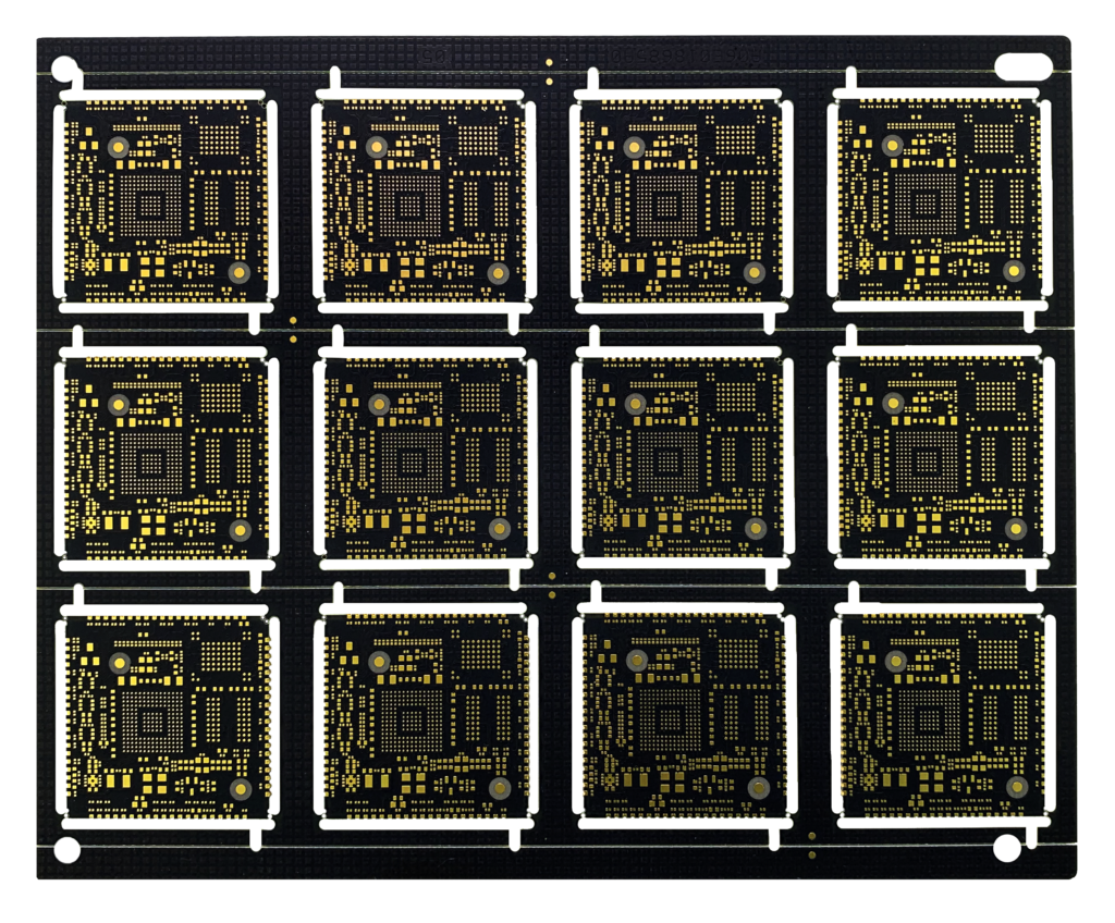
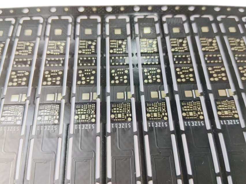
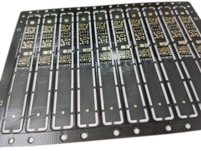
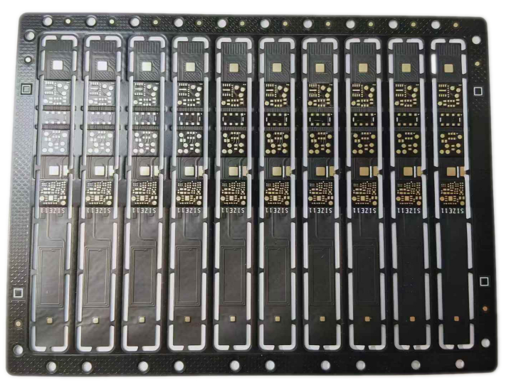
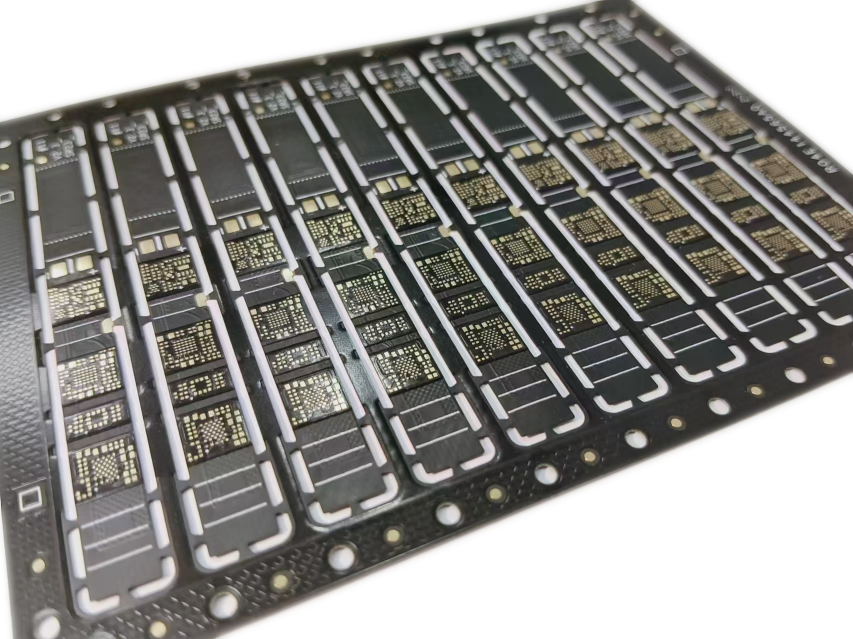
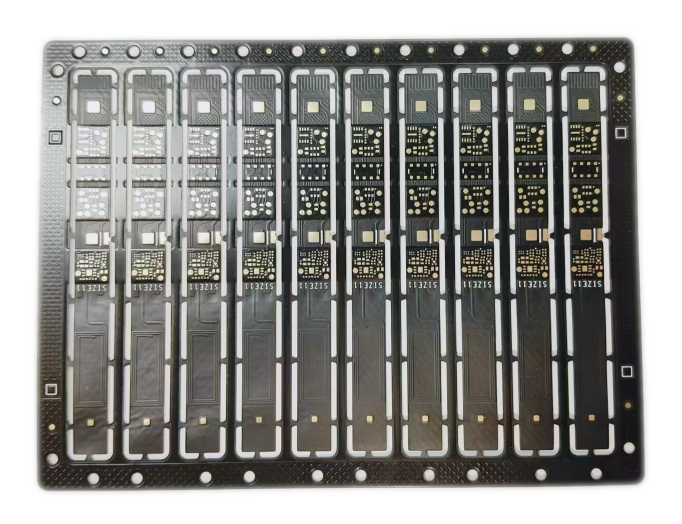
Our Multi-layer PCB Case
Multilayer FPC
Application: Smart Ring
Layer Count: 4 Layer
Material: PI+FR4
Board Thickness: 0.35 MM
Min Trace 3/3mil
Min BGA 8.7mil
Min Hole 0.1mm
Surface Treatment Immersion Gold 2u’
Board Size 72mm*6.5mm
Panel Size 114.6mm*86mm/10pcs
Solder Mask Matte Black
Blind Holes L1-L2 0.1MM, L3-L4 0.1MM
Buried Holes L2-L3 0.2MM
Why Choose Us
Competitive Pricing
More than a decade of experience in the PCB industry ensures quality components at competitive prices.
Fast and reliable delivery
Partnership with multiple global logistics providers ensures timely and reliable shipping.
Quality Assurance
A dedicated quality control team conducts manual visual inspections to ensure all products meet strict quality standards.
We have many international certifications:
We also hold several international quality certifications:
●IATF 16949:2016
●ISO 9001:2015
●ISO 45001:2018
●UL
At the same time, we are always committed to environmental protection. We have an environmental management system certification to ensure that our manufacturing process is environmentally friendly and sustainable.


Frequently Asked Questions(FAQ)
- What is the maximum layer count for your Multi-Layer PCBs?
We manufacture up to 40-layer PCBs with advanced lamination techniques.
- Can you provide impedance-controlled Multi-Layer PCBs?
Yes! We offer custom stack-up designs for controlled impedance applications.
- How can I get a quote for Multi-Layer PCBs?
Contact us with your design files, and we will provide a quote within 24 hours.
Application areas