
How do we perform aluminum PCB manufacturing?
Aluminum PCB is a common type of PCB. Recently, we contacted a group of users who need aluminum PCBs, and they all asked us how to manufacture aluminum PCBs. We will make a unified reply here and answer you in detail about our aluminum PCB manufacturing so you can confidently cooperate with us.
The first step in aluminum PCB manufacturing is the design and layout.
Our first step in aluminum PCB manufacturing is design and layout, during this stage engineers use CAD software to create the PCB layout, considering factors such as component placement, signal routing, and thermal management. Signal integrity is another important factor when designing aluminum PCB manufacturing, and our engineers carefully route the wiring to minimize signal distortion, electromagnetic interference (EMI), and crosstalk. Also, adhere to best impedance matching, signal grounding, and signal integrity analysis practices. The materials and manufacturing techniques involved in the design and layout process will meet the required performance standards.

The next step in aluminum PCB manufacturing is substrate preparation!
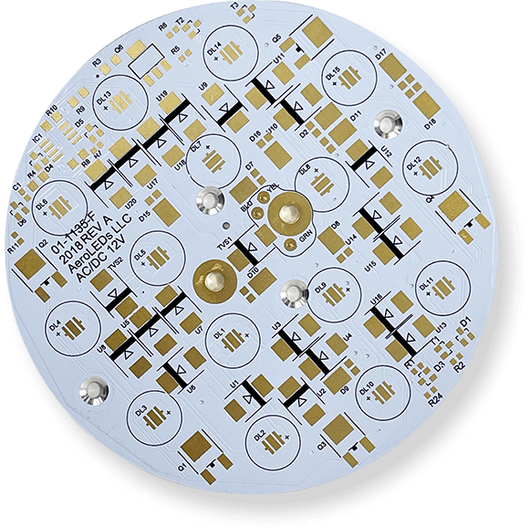
After the design is complete, the next step is substrate preparation. The substrate typically consists of thermally conductive dielectric material sandwiched between layers of aluminum or aluminum alloys. Substrate preparation begins with selecting a high-quality aluminum plate or panel that meets the required thickness, conductivity, and surface finish specifications. These aluminum substrates undergo rigorous testing and inspection to meet strict quality standards. We then apply a thermally conductive dielectric layer to the aluminum substrate to provide electrical isolation while promoting efficient heat transfer.
The third step in aluminum PCB manufacturing is copper cladding!
Once the substrate is ready, we apply a thin layer of copper on both sides of the aluminum core. This copper layer acts as a conductive path for electrical signals and components. The prepared aluminum substrate is then coated with a thin layer of copper through a process called lamination or bonding. During the lamination process, we use heat and pressure to carefully bond sheets of copper foil to the surface of the aluminum substrate. This ensures a strong and uniform bonding between the copper and aluminum layers, laying a solid foundation for the next etching and patterning process.
The fourth step is etching and imaging!
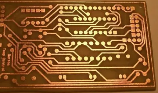
We first apply a layer of photoresist material to the substrate and then expose it to UV light through a photomask with the desired circuit pattern. During this process, the photoresist undergoes chemical reactions, and developers subsequently remove it, leaving the desired circuit pattern on the surface of the copper-clad aluminum substrate. The next step is etching, where we use a chemical etchant to selectively remove the exposed copper areas, leaving the desired conductive paths and circuit traces on the substrate. Finally, we strip the remaining photoresist material from the substrate, leaving a clear circuit pattern on the copper-clad aluminum surface.
Step 5 Drilling and Plating
We drill precision holes into the aluminum PCB and copper layers to act as conduits for electrical connections between the different layers of the aluminum PCB. We use other high-precision drilling equipment, such as CNC drill machines, to achieve precise hole sizes and locations while maintaining tight tolerances. Next, we perform electroplating, wherein we immerse the drilled PCB in a plating solution containing dissolved metal ions, and we apply an electric current to promote metal deposition onto the exposed surface. Throughout the drilling and plating process, we use automated inspection systems to verify the accuracy of hole size, location, and plating thickness while performing visual inspections and electrical tests to check for defects.
The final step is solder mask application, finishing and testing!
The final step is applying a solder mask on the aluminum PCB. A solder mask protective layer is applied to the PCB surface to cover the copper traces and pads and protect them from oxidation and contamination. This is followed by additional surface treatment of the aluminum PCB, including surface treatments such as HASL, ENIG, OSP, and immersion silver. Finally, we will conduct comprehensive testing and inspection of the aluminum PCB using electrical, visual, and functional testing to ensure compliance with specifications. We can only deliver high-quality products to customers.
Ultimately
Our aluminum PCB manufacturing involves a series of complex steps, from initial design layout to substrate preparation, copper pouring, etching, drilling, electroplating, solder mask to final finishing and testing, we ensure at each stage that we can produce high-quality aluminum PCBs.