
How do we avoid board bending and warping during TG170 PCB manufacturing?
When doing PCB manufacturing, ensuring the board’s structural integrity is essential. For the TG170 PCB to be high-temperature resistant and durable, the board must be prevented from bending and warping during manufacturing. This is also a question that many users will ask us: How can we avoid board bending and warping in TG170 PCB manufacturing? This article will discuss various strategies and best practices for you.
Use suitable TG170 PCB material to avoid bending and warping!
One of the main factors that causes PCB bending and warping is the coefficient of thermal expansion (CTE) mismatch between the various layers of the board. The materials used in the TG170 PCB construction expand or contract at different rates when the temperature changes, causing mechanical stress and deformation. Therefore, we want to use materials with compatible CTEs to reduce this mismatch and the risk of bending and warping. At the same time, we also need to understand the material properties of TG170 PCB. Choosing materials with high Tg values is crucial to prevent PCB bending and warping, especially in environments with common temperature fluctuations or thermal stress.
Optimizing design for manufacturability when performing TG170 PCB manufacturing
In addition, layout and routing also need to be considered when manufacturing TG170 PCB. We want to reduce the complexity of the PCB layout, reduce the number of vias and blind/buried vias, and optimize trace width and spacing to simplify the manufacturing process and improve signal integrity. In addition, choosing the right materials and stackup configuration can also optimize the manufacturability of the TG170 PCB. Choosing consistent performance materials ensures uniform thermal performance and reliable processing during the manufacturing process. Optimize layer stacking to minimize signal crosstalk, impedance changes, and warpage.
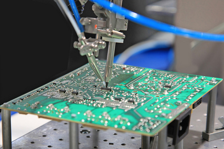
Controlled lamination process used in TG170 PCB manufacturing
During TG170 PCB manufacturing, we mitigate bend and warp by employing a controlled lamination process where we carefully control the temperature, pressure, and duration of the lamination cycle to achieve optimal bonding between the layers of the PCB stack-up. This process reduces changes in material properties, reduces internal stresses, and prevents PCB layers from delaminating or splitting, which could lead to bending, warping, or other mechanical issues. In a controlled lamination process, we subject a PCB stack of multiple layers of copper foil, prepreg, and core material to high temperatures and pressures in a controlled environment. This allows the resin in the prepreg layers to flow and bond the copper layers and core together, creating a strong, uniform structure with excellent adhesion and mechanical strength to reduce bending and warping issues.
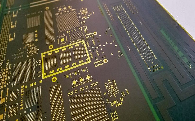
Precision drilling and milling technology
We also utilize precision drilling and milling processes to improve positioning accuracy by precisely drilling holes to ensure components are correctly aligned and securely mounted. This reduces the risk of mechanical stress and deformation from bending and warping. Additionally, we employ precision milling technology to shape and contour PCB edges and remove excess material from the board surface. We use CNC milling machines equipped with high-resolution servo motors and precision cutting tools to achieve smooth, even edges and precise dimensional accuracy. Reduces uneven stress distribution and the possibility of bending or warping during subsequent processing and assembly stages.
Thermal Management Strategies
We also incorporate thermal management strategies to make controlled heating and cooling uniform during manufacturing, thereby reducing thermal gradients and ensuring uniform expansion and contraction throughout the board, preventing bending and warping due to uneven thermal stress distribution. In addition, we will incorporate heat dissipation holes and heat sinks into the design of TG170 PCB to effectively dissipate heat and reduce thermal stress accumulation. By placing thermal vias and heat sinks in key areas of the TG170 PCB, we increase thermal conductivity and reduce the risk of bending and warping.
Ultimately
To prevent board bending and warping in TG170 PCB manufacturing, we use appropriate thermal management, precision drilling, and milling techniques, as well as controlled lamination processes, and optimize manufacturability using the right materials to avoid this problem. Therefore, you can confidently cooperate with us, and we will ensure the integrity and reliability of PCB quality.