
What are the steps involved in PCB customization?
PCB customization is a key process in manufacturing electronic applications and equipment, allowing users to customize PCBs to meet specific requirements and functions. Whether you want to optimize your layout, add special features, or enhance performance, PCB customization can make it happen. In this guide, we’ll walk you through the basic steps involved in PCB customization.
Step 1: Define design requirements and goals
The first step in PCB customization is understanding your requirements and goals, which are the basis of the entire design and manufacturing process. First, the functional requirements of the PCB are determined, including electrical characteristics, signal integrity requirements, power requirements, and any features or functions. For example, automotive applications are required to withstand high temperatures vibrations and in consumer electronics devices they may need to meet strict size and weight constraints.
Step 2: PCB customization design and layout
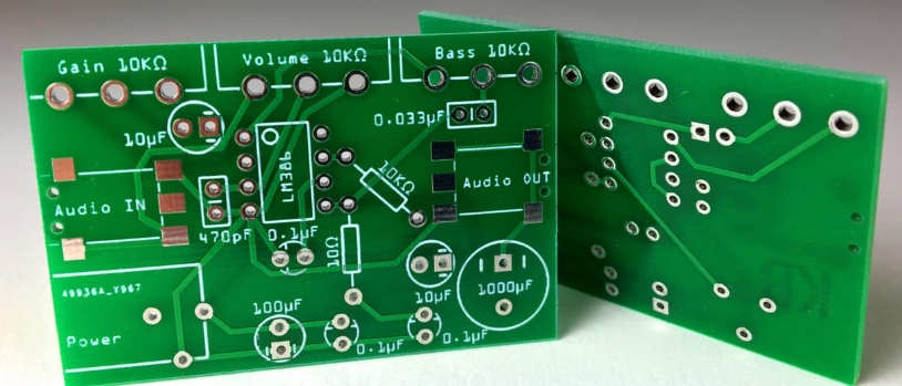
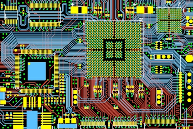
After determining your design requirements and goals, the second step in PCB customization is the layout, translating your requirements and goals into a suitable layout. Typically, PCB designers must use specialized CAD software to create schematic diagrams representing the PCB’s electrical connections, components, and circuits. Next, convert the schematic into a physical layout. The designer places the components on the PCB at this stage and lays out the electrical traces. Once components are placed, consider connections between traces while ensuring factors such as signal integrity, impedance control, and EMI mitigation.
PCB Customization Step 3: Prototype Development and Testing
The third step in PCB customization is prototype development and testing. Prototype development first manufactures small batches of PCBs based on the previous design and layout. Once the PCB prototype is completed, it is assembled and electronic components such as resistors and capacitors are mounted on the board. Use SMT for assembly according to design requirements. Once assembled, the prototype PCB undergoes extensive testing and validation to evaluate its electrical performance, functionality, and reliability. to verify the functionality of the PCB and ensure that all electrical connections are intact. This includes continuity testing, voltage measurements, signal integrity scores, and more. We perform functional testing to verify that the PCB operates as expected and meets specified requirements and goals.
PCB customization step 4: mass production manufacturing
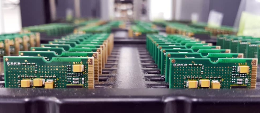
The fourth step in PCB customization is to mass-produce PCBs. Mass production can begin after the PCB prototype is successfully verified. The first stage of mass production is determining the materials and components. Next, comes the conversion of raw materials into finished circuit boards. Multiple sequential steps include board lamination, etching, drilling, plating, and solder mask application. Therefore, we can adopt automated equipment and precision manufacturing technology to ensure the accuracy of the entire manufacturing process. After PCB manufacturing is completed, SMT assembly is performed. Once assembly is complete, a visual inspection of the AOI is performed to detect any defects, welding issues, or assembly errors. Then, electrical testing, functional testing, and other tests are conducted. Finally, the finished PCB is packaged, labeled, and shipped to customers.
Step 5: Post-production support and maintenance
Even after the custom PCB is delivered, the process does not end. Documentation is important when we complete a custom PCB project as this ensures easy access to key information when needed and facilitates efficient maintenance and repair activities. Additionally, post-production support includes the ability to provide technical support and troubleshooting guidance should you encounter custom PCB issues. This includes diagnosing problems, determining root causes, and providing solutions.
In general
PCB customization is not complicated, but you must know your design requirements and goals. In this guide, we provide a customized step-by-step process that you can reference. As a PCB manufacturer, almost every project we come into contact with involves customized functions, which shows the importance of customization.