Copper Filling Techniques for Vias in 2 layer heavy copper PCB
As we face different customer needs, technology development has created a 2 layer heavy copper PCB, mainly to provide enhanced functionality for high-power applications. In 2-layer heavy copper PCBs, using through-hole copper filling technology plays a key role. This article reveals the importance of 2-layer thick copper PCBs and looks at advanced copper filling techniques for vias.
Learn about 2 layer heavy copper PCBs
2 Layer heavy Copper PCB A uniquely constructed circuit board with two layers of copper traces and a copper thickness that exceeds standard sizes. The increased copper thickness enhances the board’s current-carrying capabilities and thermal conductivity, making it suitable for high-current applications. They can handle high currents without significant voltage drops or excessive heat generation. This makes them ideal for power electronics, motor drives, automotive applications, and other scenarios where large amounts of power must be transmitted efficiently. The increased copper thickness directly contributes to lower resistance, reducing the risk of overheating and voltage loss. The design minimizes the effects of resistive losses, ensuring that the power delivered closely matches the intended output.
The Nature of Vias in 2 Layer heavy Copper PCBs
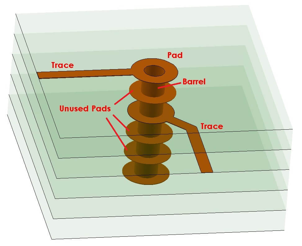
Vias in 2 layer heavy copper PCBs serve as conductive paths, bridging the connection gap between the board’s top and bottom copper layers. Vias are vital in creating a continuous electrical path between the top and bottom copper layers. The board’s thick copper layer is designed to handle high-current applications, while vias help ensure seamless electrical signal and power transfer. Vias essentially act as vertical conduits, enhancing the functionality and connectivity of a 2 layer heavy copper PCB. They are critical to achieving the required electrical performance, especially in complex circuit designs where components on both sides of the board must be interconnected.

2 layer heavy copper PCB copper filling technology
The primary purpose of copper fill is to solve the challenges associated with carrying high currents across PCBs. Maintaining low resistance and efficient current flow is critical in 2 layer heavy copper PCBs designed for power electronics or other high-current scenarios. Copper fill helps achieve this by enhancing conductive paths, reducing resistive losses, and improving the board’s overall performance.
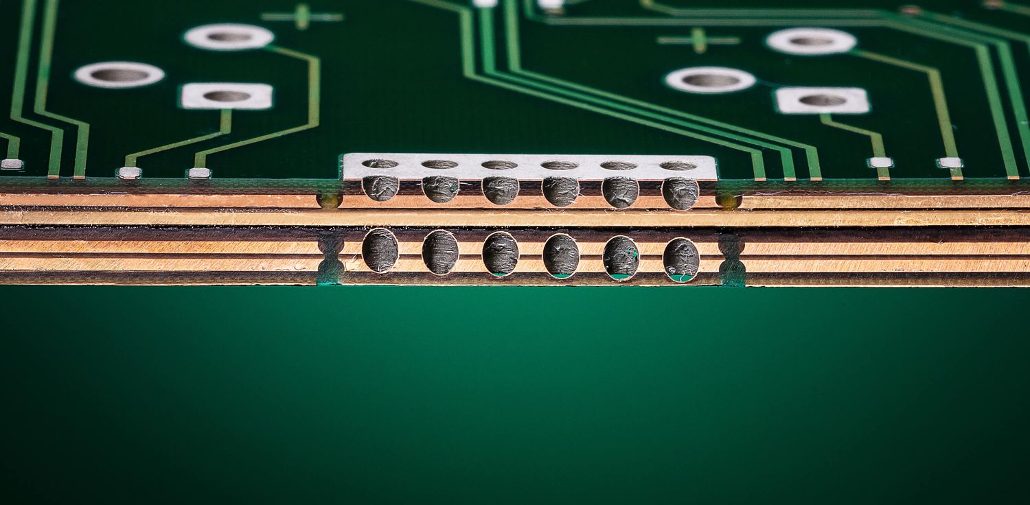
The copper filling process typically involves the application of a conductive material (usually copper) using various methods such as electroplating or electroless plating. This fills the via or via, creating a seamless connection between the top and bottom copper layers. Copper not only improves electrical conductivity but also helps improve the structural integrity of the PCB. A significant advantage of copper filling is the reduction of thermal stress and electrical resistance. The filled copper enhances the thermal conductivity of the vias and facilitates better heat dissipation.

Advanced copper plating methods
Advanced copper plating methods can enhance the performance of 2-layer heavy copper PCBs. One cutting-edge approach is using advanced plating chemistries, which involve developing and applying specialized electrolytes and additives. These formulations improve the uniformity and quality of copper plating, resulting in more consistent thickness throughout the PCB. This consistency is critical to ensuring predictable electrical performance and reducing resistance variation. In addition, advanced pulse plating technology has become a powerful method for precise copper deposition. Pulse plating involves AC pulses during the plating process, allowing for better control of the deposition rate and the ability to create a smoother, denser copper layer. This enhanced control helps reduce surface roughness and improves the overall quality of copper plating.
Challenges and Solutions
A significant challenge with 2 layer heavy copper PCBs is achieving uniform copper fill-in and vias. The uneven filling can cause copper thickness variations, resulting in inconsistent conductivity and reduced performance. Advanced techniques such as pulse plating and controlled current density distribution can be used to overcome this challenge. These methods allow precise control of copper deposition, ensuring uniform fill and reducing the risk of resistive loss.
Another challenge arises from the aspect ratio of the vias, especially in high-density PCB designs. As the aspect ratio (depth to diameter) increases, achieving full copper fill becomes more difficult. To solve this problem, we use optimized plating chemistry and methods, including additives that enhance the throwing power of the plating solution. These innovations help achieve better copper distribution within high aspect ratio vias.
Power electronics with advanced copper filling technology
The fusion of 2 layer heavy copper PCBs with advanced copper fill technology marks the ability to accommodate high-current applications. This innovation enables designers and engineers to push boundaries and usher in a new era of connectivity, efficiency, and reliability in electronic devices.

