
The Advantages of Using 2 Layer PCBs in Green Solder Mask
Many 2-layer PCBs we often see have green solder masks. There are many advantages to using 2 Layer PCBs in Green Solder Mask. From appearance to improved signal integrity, what are their advantages we will detail in this article?
2 Layer PCBs in Green Solder Mask: Optimum Signal Integrity and Performance
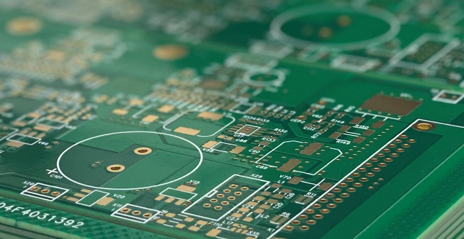
2 Layer PCBs in Green Solder Mask are the best choice for achieving superior signal integrity and performance in electronic applications. Because the green solder mask is the protective layer that covers the copper traces on the PCB, it serves multiple functions. It helps improve the reliability and efficiency of the board. Regarding signal integrity, 2-layer PCB designs offer advantages for many applications. The simplicity of the two-layer stack minimizes signal interference. It allows for impedance control, and the green solder mask provides insulation and protection from environmental factors such as moisture, dust, and contaminants.
2 Layer PCBs in Green Solder Mask: Cost-Effective Manufacturing and Assembly
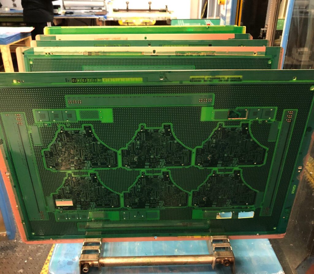
2 Layer PCBs in Green Solder Mask facilitate visual inspection of the PCB during manufacturing and assembly. The high contrast that green can provide helps quickly identify traces and components, and since there are only two layers of copper traces, manufacturing, and assembly steps become more straightforward than with multilayer boards. This significantly reduces manufacturing costs, making 2-layer PCBs a cost-effective choice for various applications. The insulating properties of the green solder mask provide essential protection for the copper traces from environmental factors, reducing the risk of short circuits and improving PCB reliability.
Reliable thermal management
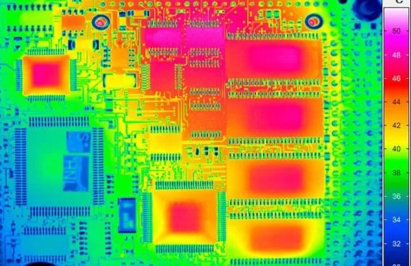
They contribute to reliable thermal management in electronic devices. Green solder mask exhibits good reflectivity in the infrared spectrum, helping to minimize heat absorption. This characteristic is essential in electronic devices, where effective thermal management is crucial to prevent overheating and ensure the longevity of components. The 2 layer PCB design lends itself to efficient heat dissipation. Having copper traces on both the top and bottom layers enables the PCB to distribute the heat generated by the electronic components more efficiently. This allows for better thermal conductivity and reduces the risk of localized hot spots, which can negatively impact the performance and reliability of the device.
Application Versatility
In consumer electronics: 2 Layer PCBs in Green Solder Mask are widely used in consumer electronics devices such as smartphones and tablets. At the same time, these PCBs can be used in industrial equipment and machinery, including control systems, automation equipment, and sensors. The green solder mask’s durability and thermal management capabilities make these PCBs suited for the harsh conditions of industrial environments. They are also more suitable for automotive electronics, including engine control units and entertainment systems.
Easy to troubleshoot and maintain
The green color of the solder mask provides high contrast to aid in visual inspection during manufacturing, assembly, and maintenance. Designers and technicians can quickly identify traces, components, and potential issues. Plus, the simplicity of a 2-layer PCB design makes it easier to inspect and identify components. Reducing the number of layers simplifies the circuit’s complexity, enabling technicians to quickly locate and resolve potential faults. If return repairs are required, the green solder mask simplifies the repair process.
Ultimately
The article shows us that their advantages are efficient manufacturing and assembly, reliable thermal management, application versatility, etc. These advantages enable designers and manufacturers to better design PCBs suitable for various applications.