
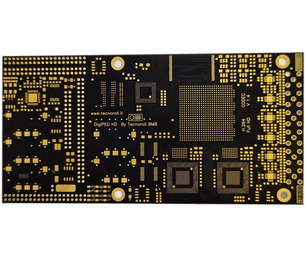
What functions does 300 G high speed PCB have?
300 G high speed PCB can meet the pursuit of faster and more efficient data transmission in many electronic communication equipment. In this article, we will explore the multifaceted capabilities of 300G high-speed PCBs and illustrate their critical role in powering electronic devices and communications systems. In addition to facilitating lightning-fast data transfer, 300G high speed PCBs are crucial in advancing 5G infrastructure.
Core Features of 300 G high speed PCB
The core function of 300G high speed PCB is to achieve unprecedented data transmission speeds. 300G high-speed PCBs are designed to handle extremely high frequencies, meeting the demands of 300G data rates and minimizing signal loss and distortion. They are specifically optimized for low latency, reducing delays in data transfer. This is critical for applications where real-time data processing is vital. They use specialized routing techniques to manage high-speed signals effectively, minimize crosstalk, and ensure the integrity of data signals as they traverse the PCB. To maintain signal integrity and prevent electromagnetic interference (EMI) and radio frequency interference (RFI), 300G high-speed PCB uses effective shielding measures to ensure reliable data transmission in noisy environments.
300G High Speed PCB Optimized Signal Integrity
One of the most essential features of 300G high speed PCBs is signal integrity optimization, ensuring reliable and efficient data transmission at unprecedented speeds. Precise control of impedance matching throughout the PCB ensures signals propagate with minimal reflections and distortion, maintaining signal quality. Optimizing via design helps reduce signal discontinuities and impedance mismatches, thereby maintaining signal integrity during signal transitions. Using substrates with low dielectric loss tangent values minimizes signal attenuation, ensuring signals can travel longer distances without significant attenuation. The use of advanced dielectric materials in materials is critical to reducing signal loss and maintaining stable characteristics at higher frequencies.
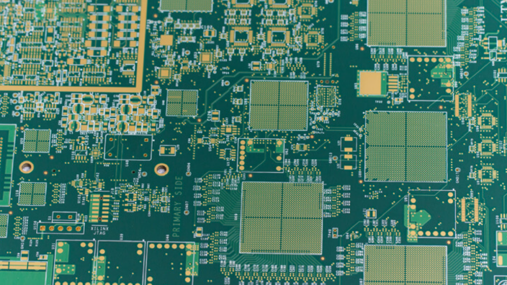
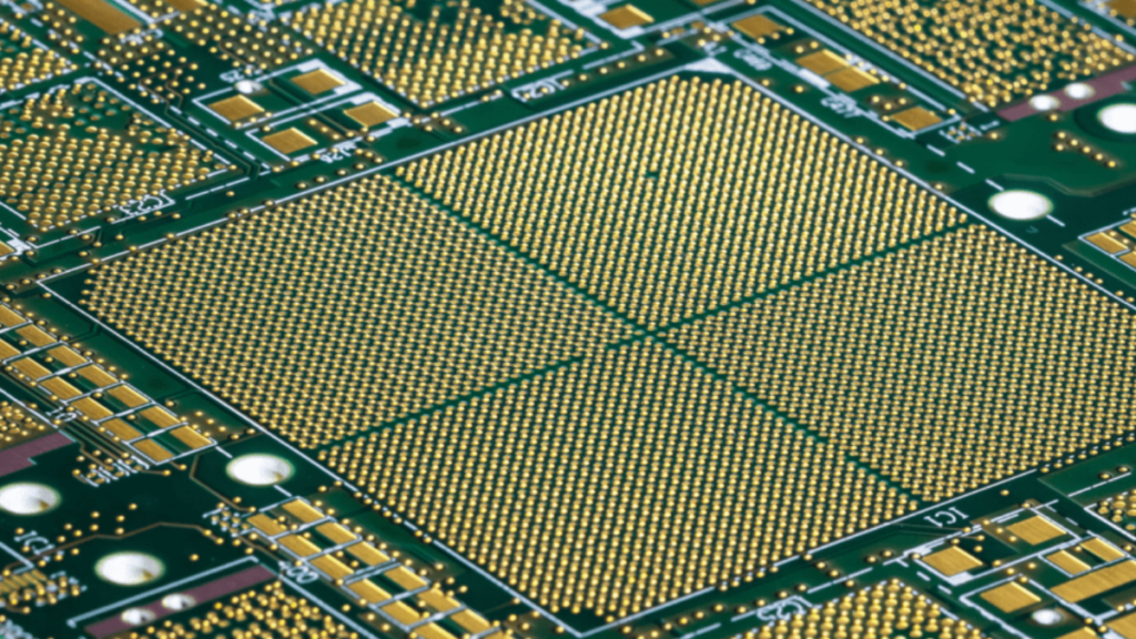
Facilitate high-density interconnection
300G high speed PCBs go beyond speed and integrity to facilitate high-density interconnects. 300G high-speed PCBs employ HDI design principles involving techniques such as laser drilling and sequential lamination, enabling the creation of complex, high-density interconnects. Differential pair routing, controlled impedance routing, and optimized trace geometry minimize crosstalk and signal attenuation to ensure a stable connection. Vertically stacked microvias provide additional routing options in high-density areas, enabling efficient interconnection of components and enhancing design flexibility. By facilitating high-density interconnects, 300G high speed PCBs would allow designers to integrate more functionality into smaller spaces.
Advanced materials for enhanced thermal management
Reliability is a cornerstone feature of 300G high-speed PCBs, and advanced thermal management is a core element in achieving this reliability. They often feature cutting-edge materials with excellent thermal conductivity properties to dissipate heat and effectively prevent thermal issues affecting performance. Optimal thermal management is critical for the reliability of electronic systems in different environments under different temperature conditions. Careful consideration of materials and thermal design highlights the 300 G high-speed PCB’s ability to deliver reliability in mission-critical applications.
300G high speed PCB empowers 5G infrastructure
300G high speed PCBs also enhance 5G infrastructure by providing necessary support for advanced communications and data transmission requirements. Their 300G data transmission rate enables ultra-fast data transmission and supports the high bandwidth requirements of seamless 5G network connections. Ensures signal integrity, critical for high-frequency 5G signals, minimizing signal loss and distortion during massive data transmissions. They facilitate the integration of advanced antenna systems, enabling the deployment of massive MIMO configurations to enhance network coverage and capacity. They support millimeter wave frequencies, enabling high-frequency bands to increase network capacity and data rates, a key component of 5G technology.
Summary review
We have seen in 300G high-speed PCB the ability to empower 5G signals. The ability to optimize complete signals can also promote high-density interconnection. If you want to keep your communication equipment up to date, then 300 G high-speed PCB is the most suitable.