
Addressing Wear and Tear in Hard Gold Plating PCB
Increasing the wear resistance of hard gold plating pcb requires a detailed understanding of the problems caused by wear. In this comprehensive guide, as our users continue to demand more excellent reliability and longevity from their electronic devices, mitigating wear becomes a critical aspect of designing rugged hard gold-plated PCBs. We will discuss the complexities of maintaining the luster of hard gold-plated PCBs and provide valuable solutions for PCB engineers.
Basic knowledge of wear mechanisms of hard gold plating pcb
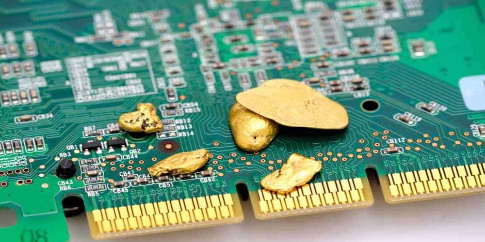
A higher gold content characterizes hard gold and is often used in critical areas of PCBs for its durability. One of the main mechanisms is abrasive wear caused by mechanical contact. Over time, repeated plugging and unplugging of connectors or other components can cause microscopic wear on the hard gold surface. Contact forces, material hardness, and contaminants affect this wear.
Fretting wear occurs in areas where there is slight oscillatory movement or vibration. This can lead to wear debris formation and microscopic activity at gold-plated contact points. Additionally, while gold is highly resistant to corrosion, exposure to harsh environmental conditions, contaminants, or chemicals can cause decay. This corrosive wear can compromise the integrity of the gold plating and affect its conductivity.
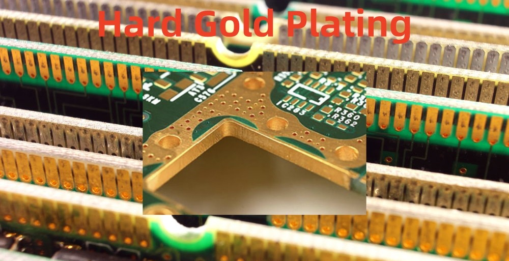
Choosing the right hard gold plating thickness for enhanced durability
Evaluate electronic components for their intended use. For frequently mated and unmated connectors, a thicker gold plating is recommended to withstand abrasive wear. High-wear environments, such as those in aerospace or automotive applications, may benefit from increased thickness. Judging the effect of gold plating thickness on electrical conductivity, thinner layers can provide improved electrical performance, especially in high-frequency applications, due to reduced skin effects. Production cost factors associated with gold material. Thicker gold layers require more material, increasing manufacturing costs.
Solving hard gold plating PCB wear challenges
Our PCB engineers can experiment with alloy compositions in the gold plating bath. Introducing small amounts of alloying elements, such as cobalt or nickel, can enhance the gold plating layer‘s hardness and wear resistance, mitigating abrasive wear issues. Composite materials can also be incorporated into gold plating formulations, combining gold with other materials, such as nanoparticles or polymers, to create a hybrid coating. These composite coatings increase hardness and durability. Some developments could employ multi-layer structures, in which thin layers of different materials are deposited one after the other. This approach optimizes the strengths of each layer, combining the hardness of certain metals with the unique properties of gold to create a coating that is wear-resistant and durable.
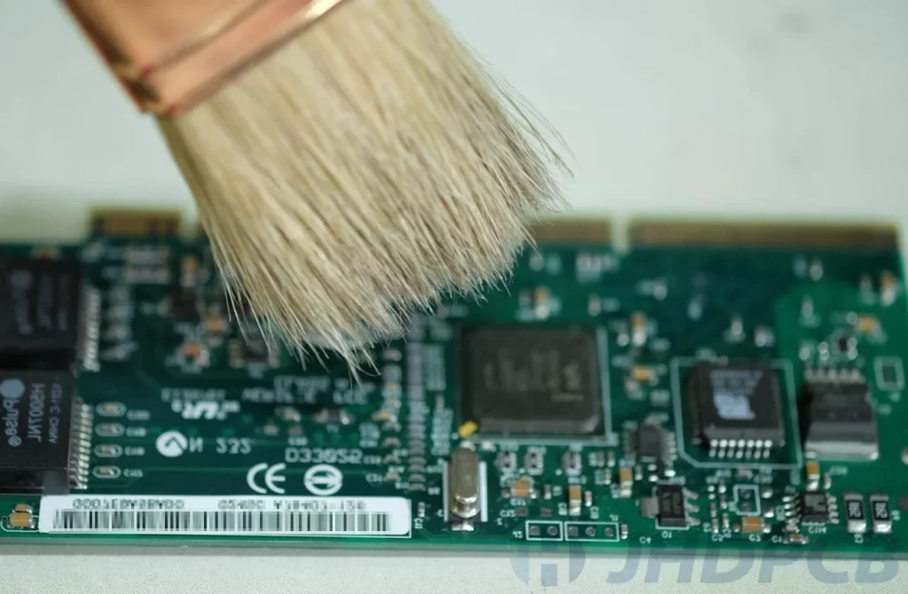
Effective Cleaning and Maintenance of Hard Gold Plated PCBs
Effective cleaning and maintenance can also reduce wear while maintaining the performance of hard gold-plated PCBs by using mild cleaning solutions explicitly formulated for electronics to avoid damaging the gold plating. Mild solvents, such as isopropyl alcohol, can effectively remove contaminants without causing abrasion on hard gold surfaces. Use a soft cleaning tool such as a lint-free cloth, a brush with non-abrasive bristles, or compressed air. Maintain the integrity of the plating by avoiding the use of abrasive materials that may scratch or rub the gold surface during cleaning. Avoid using abrasive materials, harsh chemicals, or abrasive cleaning pads. These will accelerate wear and damage the hard gold layer.
Reduce wear in high-frequency and high-temperature environments!
Choosing substrates and base metals compatible with high temperatures can reduce the potential for wear and degradation in challenging environments. Consider gold plating recipes that add alloys such as cobalt or nickel to increase hardness. More complex gold alloys are more resistant to abrasive wear, making them suitable for high-frequency applications with frequent mating and unmating. Advanced thin film deposition techniques enable precise and uniform gold plating thickness. Techniques such as physical vapor deposition (PVD) or chemical vapor deposition (CVD) provide greater control over the plating process, resulting in a more consistent, wear-resistant coating. Overheating can be prevented by implementing appropriate heat dissipation mechanisms, such as heat sinks or cooling systems, thereby enhancing the durability of hard gold plated PCBs in special use cases.
Finally
Solving the problem of hard gold plating PCB wear requires a holistic approach, using targeted strategies such as innovative formulations, thickness considerations, cleaning and maintenance, and more. By taking these proactive steps, PCB engineers can ensure that their designed PCBs can withstand the test of environmental time and provide long-lasting performance in different applications.