
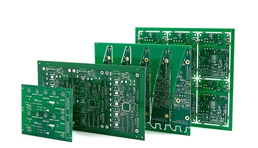
What are the common design rules for 2 layer 2oz PCB?
When designing a PCB, we must consider various factors and design rules to ensure optimal performance, reliability, and manufacturability. Specific design rules must be followed for 2 layer 2oz PCB to achieve the expected results. This guide will share the standard design rules for 2 layer 2oz PCB.
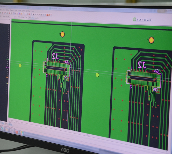
Adhere to minimum trace width and spacing
Trace width directly affects the electrical characteristics of the PCB. The width of a trace determines its resistance, capacitance, and inductance, all of which play a crucial role in signal integrity and performance. In a 2 layer 2oz PCB with limited space, it is necessary to ensure the minimum trace width to maintain signal integrity and prevent signal degradation. Trace width also affects the current carrying capacity of the PCB. Narrow traces result in higher resistance, which leads to increased power dissipation and potential overheating issues. Adhering to the minimum trace width requirements ensures that the trace can safely carry the required current without exceeding its thermal limit.
In a 2 layer 2oz PCB with limited space, maintaining adequate trace spacing can reduce crosstalk and ensure signal integrity. The spacing between traces also provides insulation and dielectric strength, preventing unintended electrical connections and shorts.
Through-hole Design and Layout Rules for 2 layer 2oz PCB
Visas are essential to PCB design, providing electrical connections for different board layers. For 2 layer 2oz PCBs, proper through-hole design ensures secure mounting and reliable mechanical support for components, which improves the durability and lifespan of the 2 layer 2oz PCBs. Manufacturers often use through-hole components in applications that require high power handling capabilities, such as power supplies, amplifiers, and industrial control systems. Effective through-hole design facilitates efficient heat dissipation and current flow.
Proper component placement is critical to optimizing signal integrity, thermal management, and manufacturability. Strategically placing through-hole components reduces signal distortion, ensures adequate space for routing, and promotes efficient heat dissipation. Thoughtful placement of components with high-frequency signals or thermal considerations mitigates potential interference or heat buildup.
Component Layout and Orientation for two layer 2oz PCB
Proper component layout reduces signal distortion, crosstalk, and EMI. Place components appropriately to minimize signal path length, impedance mismatch, and signal coupling, ensuring robust signal integrity and performance. Group components with related functions or signal paths to minimize trace length, reduce signal interference, and simplify routing.

Functional groupings enhance signal integrity, ease of troubleshooting, and scalability of modular design, facilitating efficient 2-layer 2oz PCB layout and optimization. Orient polarized components appropriately to ensure functionality and prevent assembly errors. Additionally, position components with specific orientation requirements accordingly to align with user interfaces or external connections.
Power and Ground Plane Design
Strategically lay out the power and ground planes of a 2 layer 2oz PCB to minimize signal loop area, reduce impedance discontinuities, and optimize decoupling capacitor placement. Balance and symmetrical distribution of the power and ground planes to ensure uniform current distribution and minimize voltage differences across the PCB. Size the power and ground planes appropriately to accommodate current requirements, reduce voltage drops, and provide low impedance. It is best to use thicker copper layers (such as 2oz copper) for the power and ground planes to reduce resistance and increase current carrying capacity, improving overall performance and reliability. Dedicated vias or traces should also be used to connect to all components that require power or ground connections.
Design for Manufacturability and Testability
Targeted component placement is critical to optimizing manufacturability and testability. Components should be arranged to minimize assembly errors, reduce soldering defects, and facilitate component placement and soldering process automation. Critical component placement should prioritize accessibility and ease of testing. Trace routing and spacing directly impact manufacturability and testability as they affect signal integrity, manufacturability, and accessibility of test probes. Trace width and spacing must also meet manufacturing tolerances and industry standards to ensure a reliable manufacturing and assembly process.
Achieve Perfect PCB Design
By adhering to factors such as line width and spacing, design and placement, component placement and orientation, power and ground plane design, and design for manufacturability and testability, designers can create high-quality, reliable 2 layer 2oz PCBs that meet their specific application needs.