
What is the difference between a 2 layer HAL PCB and a multi-layer PCB?
PCB is an important component that connects various electronic parts. Among the many different types of PCBs, 2 layer HAL PCB and multi-layer PCB are the PCBs that many people choose because of their specific applications and advantages. As a company specializing in manufacturing a 2 layer HAL PCB, we will tell you the main differences between these two types of PCBs.
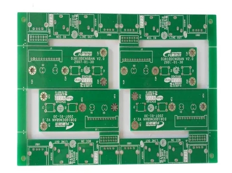
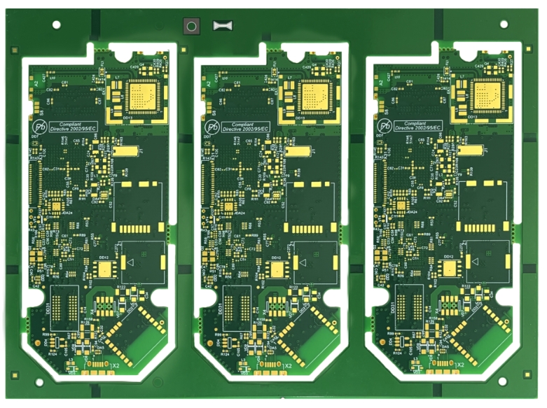
What is 2 layer HAL PCB?
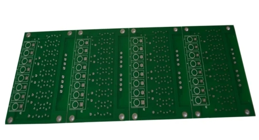
2 layer HAL PCB consists of two conductive copper layers separated by an insulating substrate in the middle. HAL refers to the hot air leveling process, which coats the copper surface with a solder layer to prevent oxidation and improve solderability. The design of 2-layer HAL PCB is simple and straightforward, which is very suitable for applications with simple circuit design. Its double-layer structure can easily route electrical signals and reduce the possibility of signal interference. The hot air leveling process ensures that the solder coating is uniform, thereby improving the durability and performance of the PCB. Their main advantage is their cost-effectiveness. Compared with multi-layer PCBs, only two layers of copper are used, and the manufacturing process is simpler and requires fewer materials.
What is a multi-layer PCB?
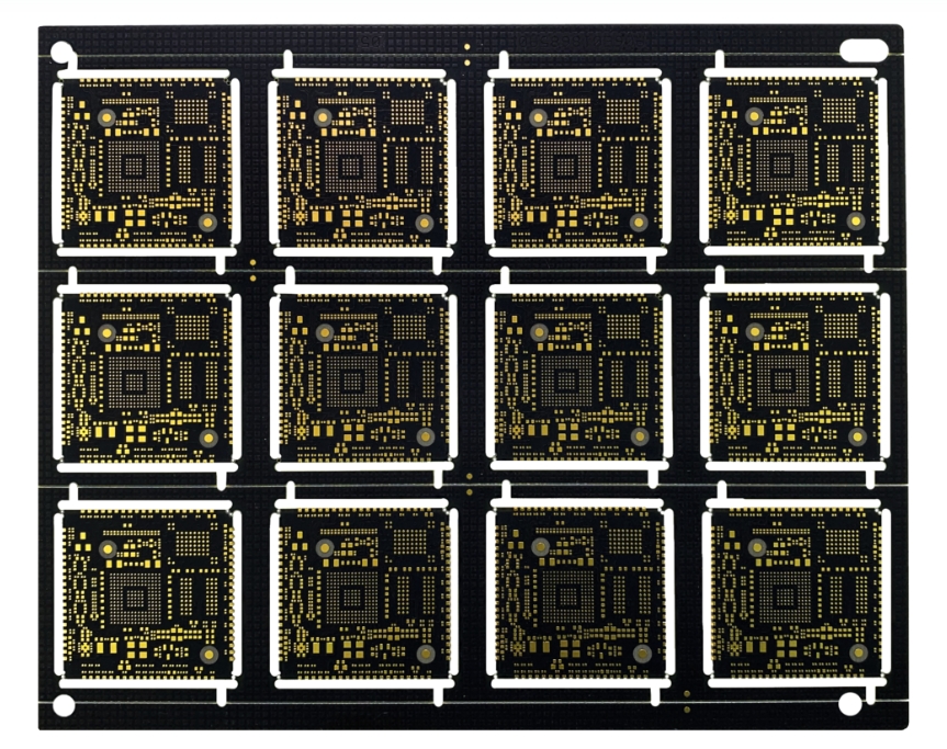
Multi-layer PCB consists of more than two layers of conductive copper separated by an insulating layer in the middle. These PCBs can have three, four, or even more layers, depending on the complexity of the design and application requirements. The main advantage is the ability to support complex circuits and high-density interconnects. This makes them ideal for electronic devices such as smartphones, computers, and medical devices. The additional layers provide more surface area for components and connections, allowing designers to create complex circuits without compromising performance or reliability. However, the increased complexity of multi-layer PCBs comes with higher production costs. The manufacturing process is more complicated.
Comparing Manufacturing Processes
The manufacturing process of 2 layer HAL PCBs and multi-layer PCBs varies greatly due to the number of layers involved and the complexity of the design. The process of 2-layer HAL PCBs is relatively simple and straightforward. It starts with creating the copper layer, applying a solder mask, and printing the screen. The hot air leveling process applies solder to the copper surface, ensuring a uniform and durable finish.
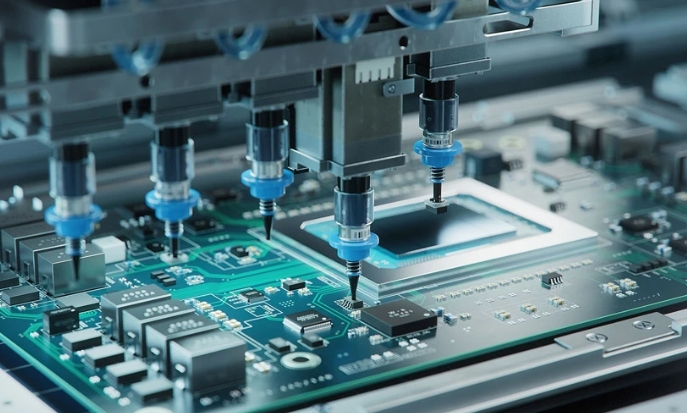
In contrast, the manufacturing process for multi-layer PCBs is more complex and involves multiple steps. The process starts with creating the individual layers and bonding them under high pressure and temperature during lamination. Afterward, technicians drill and plate through holes to create electrical connections between the layers. The final steps include the application of a solder mask, screen printing, and surface treatment.
Differences in Performance and Applications
The performance and applications of 2-layer HAL PCBs and multi-layer PCBs also vary greatly. 2-layer HAL PCBs are suitable for applications that do not require complex circuits or high-density interconnections. In contrast, multi-layer PCBs are designed for more advanced applications that require complex circuits and high-density interconnections. They are often used in smartphones, computers, medical devices, and other high-performance electronic devices. The additional layers in a multi-layer PCB provide more surface area for components and connections, enabling designers to create complex circuits with enhanced functionality and reliability.
Choose the right PCB for your needs
You can choose the right PCB based on your needs, including the complexity of the design, the performance and functionality required, the budget, and the specific application. For simple, cost-sensitive projects that do not require complex circuits, 2-layer HAL PCBs are an excellent choice. Multi-layer PCBs are the first choice for advanced applications requiring high performance, complex circuits, and high-density interconnects. The additional layers provide more surface area for components and connections, allowing designers to create complex circuits with enhanced functionality and reliability. When choosing between the two, it is necessary to evaluate the application’s specific requirements and weigh each PCB’s pros and cons. You can visit our official website to consult us.
Understand the Key Differences
The choice between these two types of PCBs depends on the specific requirements of different applications, including the complexity of the design, the required performance, the budget, and the intended use. In conclusion, whether you choose a 2-layer HAL PCB or a multi-layer PCB, understanding their differences and advantages can help you optimize the performance of your electronic device.