
Customization options in 400G high speed PCB manufacturing
PCB technology is constantly evolving, and 400G high-speed PCB is very important for applications requiring high data transmission rates, such as data centers, telecommunications, and advanced computing systems. Customizing these 400G high-speed PCBs can improve performance, meet specific engineering requirements, and provide a competitive advantage. This guide will explain the various customization options available in 400G high-speed PCBs.
Custom material selection for 400G high-speed PCB
In the process of customizing 400G high-speed PCB, the first thing to consider is the selection of base material. These materials can affect a PCB’s signal integrity, speed performance, thermal management, and overall durability. Materials that meet the requirements of 400G high-speed PCB include low-loss dielectric materials that can reduce signal attenuation and dispersion, usually using hydrocarbon laminates, PTFE, and reinforced FR-4 materials.
At high data rates, the power density on a 400G high-speed PCB results in significant heat generation. Selecting materials such as ceramic-filled hydrocarbons and polyimides with high glass transition temperatures (Tg) and thermal decomposition temperatures (Td) ensures structural integrity under thermal stress. The surface roughness of copper conductors plays a critical role in signal integrity. Smooth copper foils, such as ultra-thin (VLP) and ultra-thin (HLP) copper, can reduce skin effect losses and improve impedance uniformity across the entire PCB.
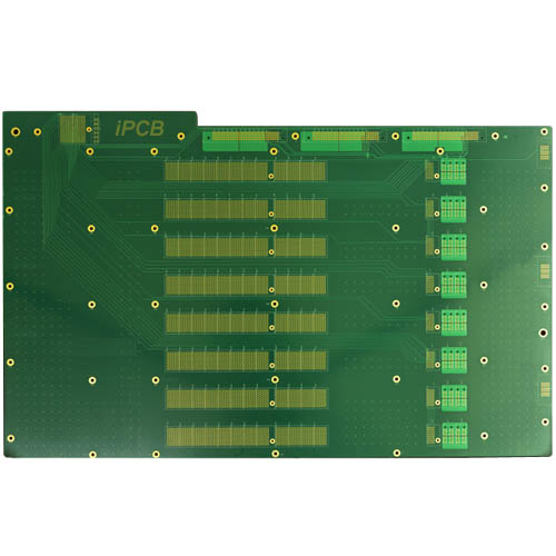
Layer configuration and stack-up design in 400G high-speed PCBs
Layer configuration and stack-up design are critical in determining the performance of 400G high-speed PCBs, especially regarding signal integrity and electromagnetic interference (EMI). You can optimize the distribution of signal, ground, and power planes by customizing the stack up to reduce crosstalk and impedance mismatch. To meet specific performance criteria, you can also use advanced technologies, such as hybrid structures involving different materials in different layers. You can fine-tune the PCB to specific operational requirements by customizing these aspects.
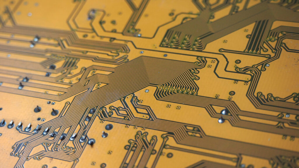
Routing and space customization
In high-speed PCBs, the configuration of traces and space is critical. Customizing trace widths and spacing can help manage impedance and minimize signal loss, which is critical to maintaining high-speed data integrity. Routing techniques such as microstrip and stripline are available in custom options to enhance signal integrity.
Microstrip configurations place signal traces on the surface layer above the ground plane and allow for easy probing and testing, but they are more susceptible to external noise. Conversely, stripline configurations enclose the signal between two ground planes, providing better shielding and less radiation. You can adjust custom options like differential pairs, matched length traces, and controlled impedance models to meet the specific requirements of your project.
Advanced custom surface treatment options
Options in surface treatment options for custom 400G high-speed PCBs range from HASL (Hot Air Solder Leveling) to ENIG (Electroless Nickel Immersion Gold), with each option offering different benefits in terms of solderability, conductivity, and wire bondability. Advantage.
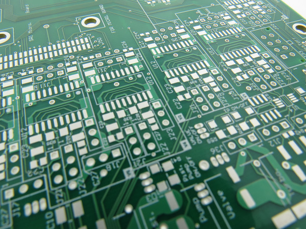
ENIG is a widely recognized surface treatment that provides excellent solderability, flat surfaces, and strong corrosion resistance, which is critical for high-frequency applications such as 400G. ENIG is also thick enough to withstand multiple reflow cycles. Immersion silver offers a cost-effective alternative with good conductivity and a flat surface suitable for fine-pitch technology. We balance cost and performance by providing excellent electrical characteristics and maintaining signal integrity at high frequencies.
Thermal management in customization options
Effective thermal management is critical to designing and operating 400G high-speed PCBs because high data rates result in significant heat generation. Managing this heat is critical to maintaining signal integrity, ensuring component reliability, and extending the product lifecycle. The basic thermal management approach involves using substrate materials with high thermal conductivity.
Incorporating thermal vias is a common method to enhance heat dissipation in PCB layers. Depending on the specific thermal and mechanical requirements, filled, capped, or plated through holes may be used. Design customization can vary the size, density, and location of these vias to optimize thermal management. Embedded cooling solutions can be integrated directly into the PCB for high-power applications. These structures provide localized cooling of critical components and are particularly effective at managing high heat loads in compact spaces.
Meet advanced needs with customization
Customization of 400G high-speed PCBs enhances performance for different applications, and by understanding and leveraging the customization options available in PCB manufacturing, users can optimize the functionality and performance of their electronic systems. As technology advances, this customization capability will become increasingly important.