
Can a 4 layer heavy copper pcb handle higher currents?
Among the many designs in PCB design, it is essential to meet customers’ needs for high-current applications while ensuring reliability and efficiency. Then, it is difficult for traditional PCBs to achieve the higher current required by modern electronic devices, leading to problems such as overheating, voltage drops, and signal attenuation. A 4 layer heavy copper pcb can solve this problem well and provide the ability to withstand high voltages for applications that require it.
Learn about 4 layer heavy copper PCBs
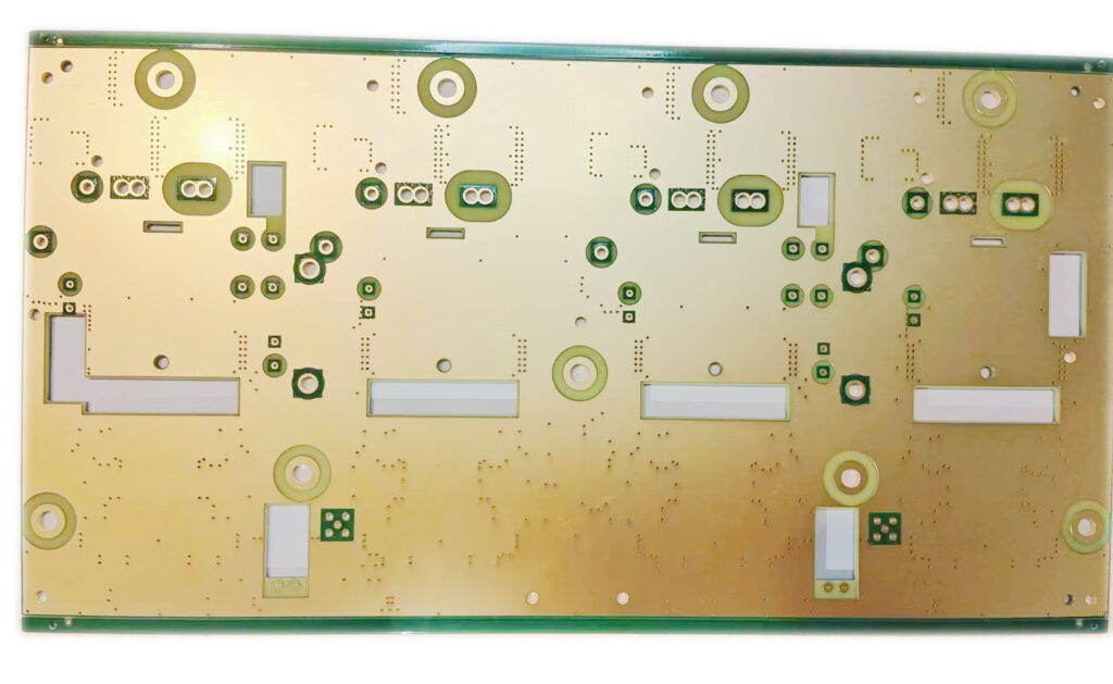
The structure of a 4 layer heavy copper pcb usually consists of four copper layers, with the two central layers typically used as power planes (positive and negative) to help distribute power efficiently throughout the circuit and shield signals on the outer layers from electromagnetic interference. The outer layer is primarily used to house signal traces, components, and other circuit elements. In thick copper PCBs, the copper thickness often exceeds the standard 1 oz/sq ft and can range to 6 oz/sq ft or more. The increased thickness enables the board to carry higher currents, provides better thermal strain tolerance, and improves the board’s mechanical strength.
4 layer heavy copper PCB enhanced current carrying capacity
One of the main advantages of 4 layer heavy copper PCBs is the enhanced current carrying capacity that allows them to handle higher currents. Its thick copper layer is an efficient conductor, reducing resistance and minimizing voltage drop even under heavy load conditions. The key to this is the increase in copper thickness. Copper thickness for standard PCBs is typically about 1 oz/sq ft, however, in thick copper PCBs the copper weight can range from 2 oz/sq ft to 6 oz/sq ft or even higher, corresponding to copper thicknesses from 70 microns to over 200 microns. Greater copper thickness allows current to flow through a larger cross-sectional area, supporting higher current levels without generating excessive heat.
Factors affecting current handling capabilities!
Several factors contribute to the current handling capabilities of a 4 layer heavy copper pcb. Of course, the most direct factor is the thickness of the copper layer. Thicker copper traces provide lower resistance, allowing efficient current flow without significant losses or degradation. In addition to thickness, the width of copper traces also has a certain impact on current capacity. Wider traces can carry more current. Designers must carefully calculate the required trace width based on expected current loads while considering allowable temperature rise. Likewise, proper spacing must be maintained between traces. Heat dissipation is also a critical factor in current handling, and overheating can cause PCB failure due to delamination, melted solder, or damage to mounted components.
For applications with high current capabilities
4-layer heavy copper PCB is widely used in high-current industries and electronic equipment, including power supplies, motor controllers, industrial equipment, automotive electronics, etc. These PCBs help increase electronic products’ performance, efficiency, and longevity by providing reliable power distribution and minimizing voltage drops. In automotive, 4 layer heavy copper pcbs are used in power converters, electric vehicle battery management systems, and high-power LED lighting systems. In industrial environments, such applications include motor drives, power inverters, and control systems for heavy machinery.

Design considerations
Several key factors must be carefully considered when designing a 4 layer heavy copper pcb, including copper thickness. The increased thickness allows the PCB to handle higher current loads by reducing resistance and the heat generated during operation. In addition to thickness, the width of the copper traces must also be wide enough to carry current without overheating. The role of stackup configuration in determining the performance of a four-layer thick copper PCB. You must use inner layers as dedicated ground and power planes for high-current applications. The choice of substrate material also affects the functionality of thick copper PCBs. Materials such as FR-4 have become standard due to their good mechanical and thermal properties and reasonable cost. However, materials such as polyimide can be selected for higher performance requirements.
Able to withstand higher currents
In summary, 4 layer heavy copper pcb provides a reliable and efficient solution for applications requiring high current handling capabilities. It has thick copper layers and advanced design features to efficiently distribute power, minimize voltage drops, and withstand heavy loads without sacrificing performance or reliability.