Email: Steven.yu@yymzhpcb.com   Telephone: 0086-13826589739

Twitter Facebook-f Linkedin-in Instagram

We are creative, ambitious, and ready for challenges! Hire Us

PCB@
  • Home
  • About Us
  • Product service
    • SSD PCB
    • Heavy Copper PCB
    • Double Side PCB
    • Multi-Layer PCB
    • Ceramic PCB
    • HDI PCB
    • Rigid-Flex PCB
    • Gold Finger PCB
    • Metal Substrate PCB
    • FPC PCB
    • SMT/DIP
    • PARYLENE Nano Vacuum Coating
  • Application Areas
  • Case
  • Blog
  • Contacts
Get a quote
PCB@
  • Home
  • About Us
  • Product service
    • SSD PCB
    • Heavy Copper PCB
    • Double Side PCB
    • Multi-Layer PCB
    • Ceramic PCB
    • HDI PCB
    • Rigid-Flex PCB
    • Gold Finger PCB
    • Metal Substrate PCB
    • FPC PCB
    • SMT/DIP
    • PARYLENE Nano Vacuum Coating
  • Application Areas
  • Case
  • Blog
  • Contacts
Menu
  • Home
  • About Us
  • Product service
    • SSD PCB
    • Heavy Copper PCB
    • Double Side PCB
    • Multi-Layer PCB
    • Ceramic PCB
    • HDI PCB
    • Rigid-Flex PCB
    • Gold Finger PCB
    • Metal Substrate PCB
    • FPC PCB
    • SMT/DIP
    • PARYLENE Nano Vacuum Coating
  • Application Areas
  • Case
  • Blog
  • Contacts

Tag: 2 layer pcb

  • Home
  • Blog
  • 2 layer pcb
Blog
2-layer PCB 11
_ December 5, 2023_ PCB@_ 0 Comments

What is the difference between 2 layer PCB and 4 layer PCB?

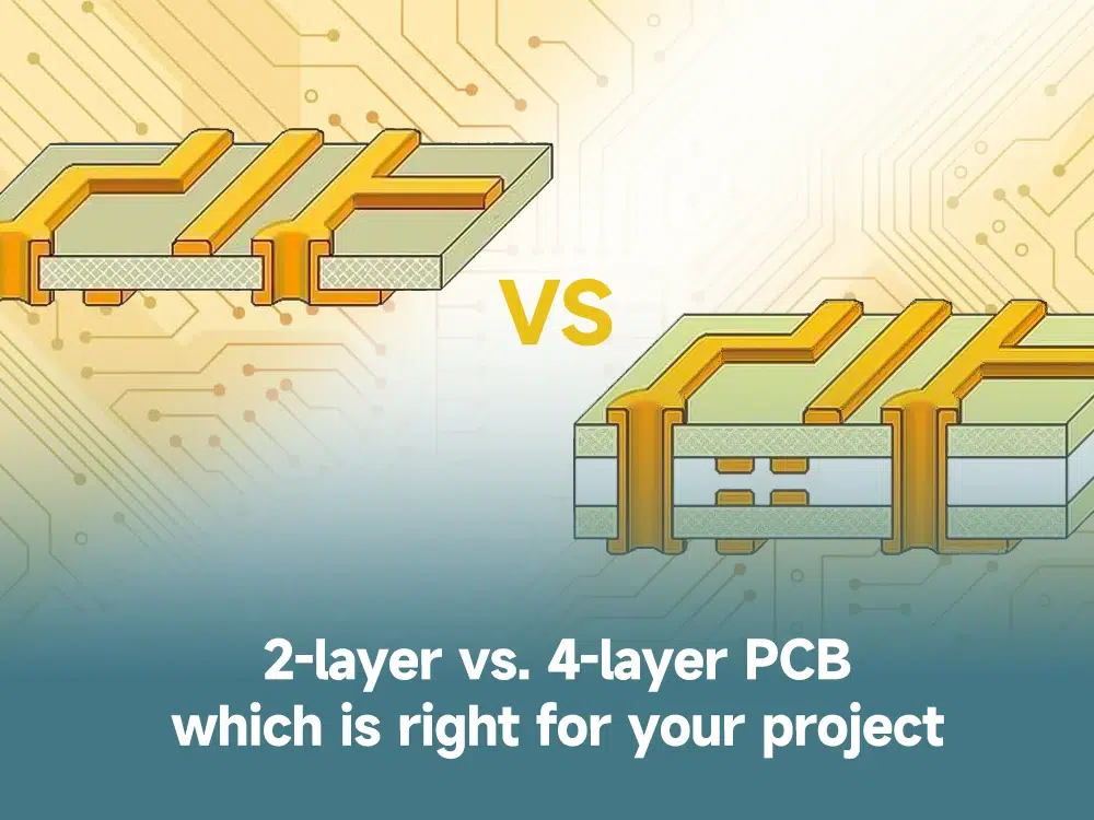
As everyone knows, in various circuit designs, the 2 layer PCB is a basic configuration characterized by two layers of copper sandwiched between insulating substrates. These layers facilitate the flow of electrical signals across the board. The emergence of 4 layer PCB allows it to handle more complex circuit designs and break through the limitations […]

LEARN MORE ♥82

Recent Posts

  • thick copper PCB for Power Reliability Engineering
  • thick copper PCB for Advanced Thermal Management
  • Metal Base PCB in Renewable Energy Applications
  • Multilayer Ceramic PCB Reliability in Extreme Conditions
  • Why Thick Copper PCB Is Critical for Power Amplifier Circuits

Recent Comments

  1. A WordPress Commenter on Master PCB Design and Manufacturing: From Concept to Reality
Categories
  • Blog (250)
Recent Posts
  • thick copper PCB
    thick copper PCB for Power Reliability Engineering
    January 22, 2026
  • thick copper PCB
    thick copper PCB for Advanced Thermal Management
    January 22, 2026
  • Metal Base PCB in Renewable Energy Applications
    Metal Base PCB in Renewable Energy Applications
    January 19, 2026
Tags
2 layer 2OZ pcb 2 layer FR4 PCB 2 layer HAL PCB 2 layer heavy copper PCB 2 Layer Immersion Gold PCB 2 layer pcb 2 Layer TG150 PCB 2 layer TG170 pcb 4 layer heavy copper pcb 6 layer SSD pcb 6-layer SSD PCB 8 layer SSD pcb 8 layer SSD PCB 8-layer SSD PCB 300 G high speed pcb 400G high speed pcb AIN Ceramic PCB aluminum oxide PCB Aluminum PCB Aluminum substrate pcb Carbon Ink PCB Ceramic PCB Double-Sided PCB double layer PCB double side PCB Gold finger FPC manufacturer gold finger pcb hard gold plating pcb HDI PCB Heavy Copper PCB Heavy Copper PCB manufacturing High frequency pcb M6 Material PCB Mid Low Loss PCB Multi-layer PCB Multilayer PCB multilayer rigid-flex pcb PCB Design power supply PCB Rigid-flex PCB Set-top box PCB smart ring flex PCB SSD PCB Thick copper pcb ultra low loss PCB