
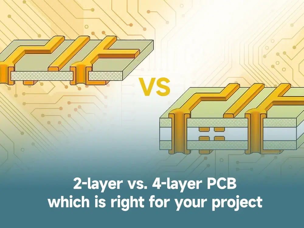
What is the difference between 2 layer PCB and 4 layer PCB?
As everyone knows, in various circuit designs, the 2 layer PCB is a basic configuration characterized by two layers of copper sandwiched between insulating substrates. These layers facilitate the flow of electrical signals across the board. The emergence of 4 layer PCB allows it to handle more complex circuit designs and break through the limitations of this layer. As these options grow, we’ll tell you more about their differences below.
Evolution from 2 layer PCB to 4 layer PCB
The board incorporates two additional copper layers in a 4 layer PCB, creating a more complex matrix for routing signals. This sophisticated performance allows for the design of denser and more complex circuits with additional layers that enhance signal integrity, reduce electromagnetic interference, and improve thermal management, making them a first choice for advanced electronic devices. As technology continues to evolve, the versatility of 4 layer PCBs paves the way for innovation in various industries. This is a feature not found in 2 layer PCBs, and the ability to create these dedicated planes can help improve signal integrity and enhance overall performance, especially in applications requiring high-frequency signals or complex electronic components.
Applications of 4 layer PCB: computer systems, communication equipment, military and avionics, etc.
Basic knowledge of 2 layer PCB
In a 2 layer PCB, limited routing space leaves management signals incomplete. Since only two layers are available, we designers must carefully plan signal paths to avoid interference and crosstalk. Their simplicity makes it very difficult to maintain optimal signal integrity, especially in high-frequency applications, and this is where the difference between Layer 2 and Layer 4 lies.
Applications of 2-layer PCB: household electronic equipment, automotive electronics, consumer electronics, etc.
Routing constraints for 2 layer PCB and 4 layer PCB
Routing is the path that signals travel on a PCB and is an important design aspect. In a 2 layer PCB, designers have certain constraints during the design process due to limited routing options. The simplicity of these boards may be beneficial for basic applications. 4 layer PCB with many routing options. The additional layers allow designers to create dedicated power and ground planes, reducing noise risk and enabling more efficient routing. The flexibility provided by 4 layer PCBs allows designers to implement complex and compact designs that are often difficult to achieve with 2 layer configurations.

Consider the cost
Because the 2 layer PCB has a simple design that reduces manufacturing complexity, thereby reducing production costs, it is a perfect choice for customers with limited budgets. However, as design requirements become more complex. 4 layer PCBs offer enhanced functionality but are more expensive to manufacture due to increased complexity and material requirements. The choice must, therefore, carefully weigh the performance benefits against the associated costs to determine the most cost-effective solution for their specific application.
Choose the correct PCB for your application
Through our sharing, we can conclude that when you need some simple electronic applications, the circuit design is simple, and the cost is limited, you can choose 2 layer PCB. If you need some applications with complex circuit design, those with high frequencies can use 4 layer PCB. The core point when selecting is to decide according to your situation. We can also provide you with more information about PCB. You can go to our official website for detailed consultation.