
High Speed SSD PCB Design Service for M.2 & NVMe
One might assume that as long as the right NAND flash memory and controller chips are selected, the circuit board design becomes naturally much simpler, ensuring the successful launch of a high-speed SSD PCB project. However, this notion is not merely incorrect; it is fundamentally flawed! A significant number of underperforming M.2 SSDs can trace the root cause of their issues directly back to the PCB itself.
In an era where data transfer rates on each PCIe lane reach as high as 10 Gbps, the circuit board is by no means a passive carrier; rather, it stands as a decisive factor in overall performance. Engineers who treat the circuit board as a mere generic component often find themselves scrambling during the late stages of the development cycle to resolve various signal integrity issues; conversely, those who truly understand the intricacies of the craft prioritise—from the very outset—ensuring that their circuit board design is absolutely flawless.
Why SSD PCB Design Fails at Speed
Standard PCB design principles don’t scale to NVMe frequencies. Three failure modes show up repeatedly at high signal speeds. First, impedance mismatch. Trace geometry, dielectric thickness, or copper weight can drift from the controlled-impedance target. At low frequencies, a 5-ohm variation is invisible. However, on a high speed SSD PCB carrying differential pairs at 10 Gbps, that same variation degrades eye diagram margin and raises bit error rate.
Second, via stub resonance. Every through-hole via has an unused stub below the signal layer. As a result, that stub acts as a resonant antenna at high frequencies — absorbing signal energy at specific frequencies. Back-drilling removes it mechanically. That’s standard practice on production SSD boards.
Third, return path continuity. High-speed differential pairs need an unbroken reference plane beneath them. Split planes and improper layer transitions interrupt the ground return path. Consequently, common-mode noise builds up and kills signal quality. Fixing this after the layout is costly. Designing for it upfront costs nothing extra.

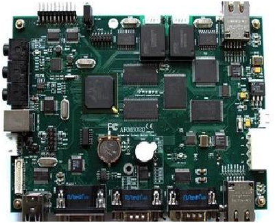
Real Specs Inside a Production-Grade High Speed SSD PCB
Material, Layer Count, and Stack-Up Decisions
Production M.2 SSD boards run at 10 layers. They’re built on FR4 TG170 material — a glass transition temperature of 170°C. That rating matters because SSDs generate significant heat under sustained writes. Moreover, a lower-rated dielectric begins to soften before the drive reaches its thermal throttle threshold. Board thickness holds at 0.85mm ±0.05mm for M.2 form factor. M.2 slot retention clips and connector specs are written around that number.
Therefore, a board 0.1mm out of tolerance creates inconsistent seating — and that shows up as intermittent connectivity in the field, not in incoming inspection. The 10-layer stack-up provides dedicated routing layers for differential pairs, isolated power planes for controller and NAND, and solid ground planes at every reference layer. Collapsing to fewer layers to cut costs is one of the most reliable ways to fail signal integrity validation.
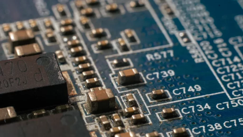
Trace, BGA, Hole, and Surface Finish Tolerances
M.2 SSD boards require 3/3 mil minimum trace and space, 8 mil minimum BGA pitch, and 0.15mm minimum drill diameter. These specs separate SSD PCB manufacturers from general-purpose shops. Surface finish is ENIG at 2μ”. It provides a flat, consistent surface for fine-pitch BGA soldering. In addition, its contact resistance is stable enough for the M.2 edge connector interface, where OSP or HASL would introduce variability. Matte black solder mask improves AOI contrast, catching defects that a green mask hides.
Panel configuration also matters. A 22mm×80mm M.2 board running 5-up on a 126mm×80mm panel needs precise V-score tolerance. Otherwise, boards that don’t break cleanly can stress BGA joints during depaneling — a defect that only appears in the field.
What a High Speed SSD PCB Design Service Should Actually Deliver
Manufacturing services and design services are not synonymous concepts. High-speed SSD PCB design services commence well before the generation of Gerber files. Pre-layout signal integrity planning establishes routing rules for differential pairs, reference plane assignment schemes, and via structure requirements.
DFM (Design for Manufacturability) reviews enable the timely detection of potential issues—such as stackup anomalies, violations in pad-to-via spacing, and copper density imbalances—before the board drilling process even begins. For M.2 SSD circuit boards, this review phase also validates the routing of PCIe channels against length-matching rules. Additionally, it verifies that the reference clock distribution scheme complies with specified jitter performance metrics. By conducting test coupon inspections for every production batch, a closed-loop management system for controlled impedance manufacturing is effectively realised.
The Manufacturing Variables That Decide Final Performance
Capability matters more than capacity. A factory running high volumes at commodity tolerances won’t consistently hit high speed SSD PCB specs. Therefore, what matters is proven process control at 3mil trace/space, back-drilling accuracy at ±0.05mm, and lot-level impedance verification with documentation.
Multi-factory operations add flexibility. They allow SSD PCB orders to route to a facility specialising in ENIG and fine-pitch processes. Consequently, prototype and production lots stay consistent — something a single generalist line can’t always guarantee. ISO 9001 and UL compliance set the baseline. The real differentiator, though, is engineering engagement. Does the manufacturer review design intent — or just Gerber files?
Build Your SSD PCB With a Team That Knows the Specs
MZH Electronics manufactures high speed SSD PCBs for demanding storage applications. Our builds include 10-layer FR4 TG170 stack-ups, M.2 form factor precision, controlled impedance fabrication, and ENIG surface finish. Moreover, our facilities in Hunan, Shenzhen, and Jiangmen maintain consistent process standards from prototype through volume production. At the design stage, our engineering team reviews your stack-up and routing requirements before fabrication begins. Gerbers already ready? We run a DFM check and return a quote within 24 hours.
Contact MZH Electronics today — and get the SSD PCB your design actually demands.