
Achieve uniform copper thickness on 4 layer heavy copper pcb
The durability and excellent current-carrying capabilities of 4 layer heavy copper PCB stem from their uniform copper thickness, ensuring that uniform copper thickness maintains their benefits and ensures reliable performance and longevity for your application. This guide will explore the steps and techniques for achieving uniform copper thickness for 4-layer heavy copper PCBs.
Basics of Uniform Copper Thickness in 4 Layer Heavy Copper PCBs
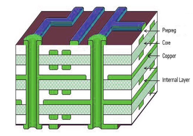
4-Layer Heavy Copper PCBs are designed to handle high currents and provide better heat dissipation than standard PCBs. These PCBs are constructed with four copper layers sandwiched between dielectric material layers. The key to their effectiveness is uniform copper thickness across all layers. In heavy copper PCBs, the copper layers are much thicker than those in standard PCBs, enabling them to handle higher currents and dissipate heat better. Uniformity of copper thickness across all layers is critical to ensure consistent electrical performance and structural integrity.
Importance of Uniform Copper Thickness in 4 layer heavy copper PCB
Uniform copper thickness ensures that electrical performance remains consistent across a 4 layer heavy copper PCB. Copper is the primary conductive material in a PCB, and its thickness directly affects electrical properties such as resistance, impedance, and current carrying capacity. Variations in copper thickness can lead to uneven current distribution, signal attenuation, and potential hot spots. These inconsistencies can cause signal integrity issues in high-speed and high-frequency applications, resulting in data loss or communication errors. Uniform copper thickness helps dissipate heat effectively, preventing hot spots that can damage components and ensuring that the PCB can withstand mechanical stress without delamination or cracking.
Design Considerations for Uniform Copper Thickness
Material selection is the foundation for achieving uniform copper thickness, and we select high-quality copper foil and laminates to ensure consistency across the substrate. Copper foil must have uniform thickness and excellent adhesion to the substrate. During the design phase, we evenly distribute copper features such as traces, pads, and pours across the board. Uneven distribution can lead to uneven copper plating, resulting in thickness variations. Designers balance the copper density of each layer to ensure that no single area is disproportionately filled with copper elements. The electroplating process is critical to achieving uniform copper thickness, requiring precise control of plating parameters such as current density, plating time, and solution composition to ensure uniform copper deposition. Uniformity can be further improved by using advanced plating techniques such as pulse plating or reverse pulse plating.
Quality Control
Quality control during manufacturing 4-layer Heavy Copper PCBs ensures uniform copper thickness. We use AOI systems with cameras and image processing software to detect copper thickness, trace width, and spacing inconsistencies. Cross-sectional analysis is also performed, which involves cutting a sample 4-layer Heavy Copper PCB and examining the cross-section under a microscope to verify copper thickness and uniformity. Electrical testing is then performed to ensure that the PCB meets performance specifications, such as resistance and continuity.

Challenges and Solutions for Achieving Uniform Copper Thickness
One of the main challenges in achieving uniform copper thickness is the inherent variability of the electroplating process. Electroplating is the most common method of depositing copper onto PCB substrates. Variations in factors such as plating solution concentration and temperature can lead to uneven deposition. To mitigate this, precise control systems and monitoring tools are used to maintain optimal process parameters throughout the electroplating cycle.
Another challenge comes from the nature of the PCB substrate itself. Variations in substrate flatness and surface roughness can affect the distribution of copper during the electroplating process, resulting in uneven thickness throughout. To address this, we use techniques such as surface treatment to create a more uniform electroplating surface.
Ensuring consistent quality and reliability
Achieving uniform copper thickness for 4-layer heavy copper PCBs is critical to ensuring their performance, reliability, and longevity. Our focus on careful design, advanced manufacturing techniques, and strict quality control measures ensure that PCBs can be produced to the highest quality and reliability standards.