
The Role of Heavy Copper PCB in Power Supply and Conversion Systems
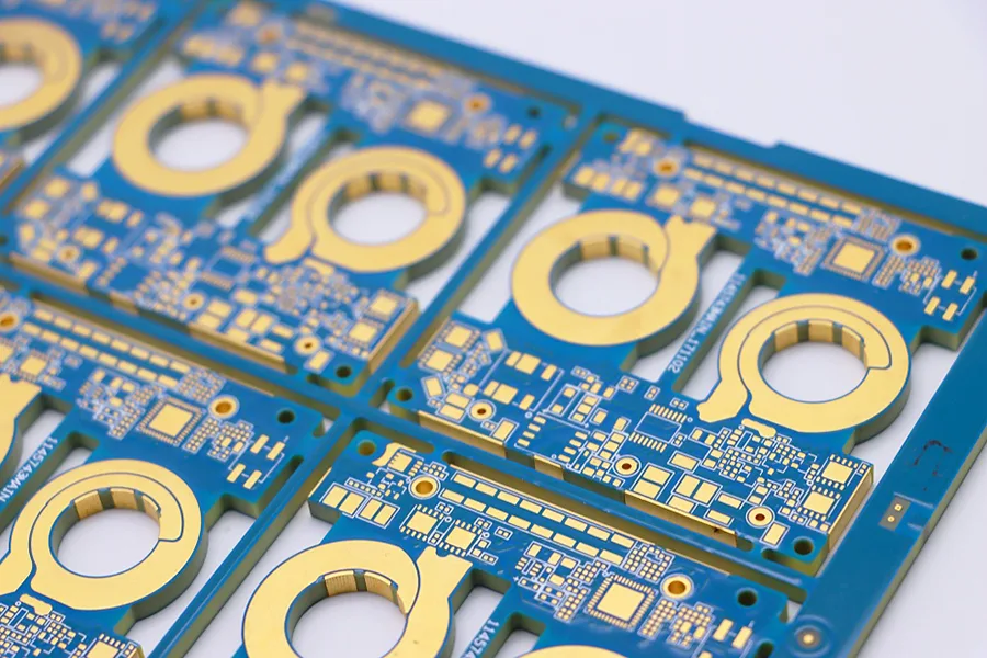
Heavy Copper PCB is critical in today’s high-power electronic applications, especially in power supply and conversion systems. These specialized circuit boards contain copper layers thicker than standard PCBs, typically over 3 oz/ft². This allows them to handle higher current loads and manage heat more effectively. These features make them ideal for converters, inverters, and power control modules that must perform under extreme electrical and environmental stress.
Enabling Higher Current Carrying Capacity
One of the most crucial features of heavy copper PCBs is their ability to carry significantly higher currents. Standard copper thickness—around 1 oz/ft²—limits current flow and increases the risk of overheating. With thicker copper traces, heavy copper boards enable more efficient power transfer and reduce energy loss across connections.
For instance, power supply units in automotive and industrial applications often require currents exceeding 20A. A regular PCB would either overheat or require larger trace widths, which consume valuable board space. A Heavy Copper PCB solves this by allowing designers to maintain compact layouts while delivering robust current-handling capabilities. This makes them essential for switch-mode power supplies (SMPS) and DC-DC converters that need to operate within small form factors without compromising performance.
Improving Heat Dissipation and Thermal Stability
Thermal management is a constant challenge in power systems. Components that process high current levels often generate heat that must be dissipated to maintain reliability. Heavy copper PCBs address this through thicker copper layers that act as effective heat spreaders. This helps reduce hot spots and prolongs the life of components.
Additionally, heavy copper traces improve the thermal conductivity of the entire circuit. They allow engineers to create a controlled and predictable thermal path when coupled with thermal vias or heat sinks. This enhances the system’s overall efficiency and reduces the need for external cooling measures. By managing thermal loads internally, systems become more compact and cost-effective—two highly desirable traits in modern electronics.
Supporting Complex Power Conversion Architectures
Power conversion systems often involve intricate circuit designs, especially in applications like solar inverters, EV chargers, and telecom power modules. These setups may require multiple voltage levels, switching components, and feedback loops. Heavy Copper PCBs allow designers to build complex multilayer layouts with power and signal integrity preserved across layers.
Furthermore, the mechanical strength provided by thick copper layers allows for secure mounting of heavy components like transformers or large capacitors. This reduces vibration-related failures and improves long-term reliability. With such robust architecture, power conversion modules can withstand both high voltage stress and environmental wear, making them suitable for mission-critical applications.
Enhancing Durability and Service Life
Durability isn’t optional in power supply systems—it’s a requirement. Systems deployed in harsh environments—like aerospace, military, or offshore energy platforms—demand materials that can withstand thermal cycling, vibration, and corrosion. Heavy Copper PCBs meet these challenges by offering superior bond strength between layers and components.
Thanks to reinforced plating via holes and edges, these boards minimize the risk of delamination or micro-cracking, common failure modes in standard PCBs. Additionally, their high tolerance for thermal and mechanical stress reduces maintenance cycles. Over time, this cuts operating costs and enhances the system’s overall reliability. It’s not just about surviving the test bench—heavy copper designs thrive in real-world stress conditions.
Compact Design Without Compromise
With increasing pressure to reduce product size, especially in portable and high-density power systems, PCB real estate becomes more valuable than ever. Heavy Copper PCBs allow space-saving designs by supporting high current loads through narrower traces and layers. This leads to more compact, efficient layouts without sacrificing power delivery.
This benefit is particularly noticeable in modular power systems or embedded industrial controllers, where internal space is limited. Engineers can route high-current paths within the board instead of scaling up the board or using external connectors. The result? Less wiring, lower resistance paths, and better EMI performance. It’s a cleaner, smarter way to build high-power systems.
Industry Adoption and Manufacturing Advances
Heavy Copper PCBs have moved from niche applications into mainstream industrial use. This shift is driven by both demand and manufacturing progress. New fabrication techniques like differential etching, high-speed plating, and advanced lamination now make producing boards with 5 oz, 10 oz, or even higher copper weights easier- and more affordable.
Moreover, quality control standards have improved. Manufacturers now offer tighter tolerances, better plating consistency, and improved layer adhesion. This gives designers more confidence to push their power supply systems harder without risking reliability. As demand grows in renewable energy, electric transportation, and data centers, the use of heavy copper PCBs is expected to rise steadily. More industries realize they can’t build the future on standard PCBs alone.
Why Heavy Copper PCB Is the Backbone of Modern Power Systems
As power systems become more compact and energy-dense, the importance of Heavy Copper PCBs will only grow. Their ability to support complex, high-load circuits in small footprints positions them as a cornerstone for innovation. If you’re designing power electronics, choosing the right PCB is not just an engineering decision—it’s business-critical. And more often than not, Heavy Copper PCB is the answer.