
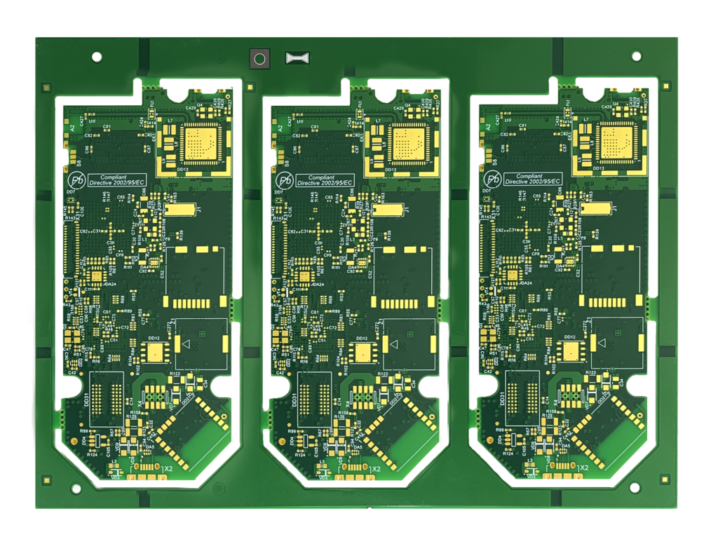
Emerging Trends and Technologies for Multi layer PCB
Multi layer PCBs have always been the most widely used in electronic design and manufacturing, and they have promoted the development of many sophisticated electronic devices. As technology advances, new trends and innovations reshape multi layer PCB design and manufacturing. This technical guide will dive deeply into the latest trends and technologies in multi layer PCB.
Advances in Multi layer PCB Materials Science
In advancing multi layer PCB materials science, an essential area of progress is the development of high-performance substrate materials for multilayer PCBs. New options such as high-frequency laminates, flexible substrates, and high-speed materials such as PTFE (polytetrafluoroethylene) and polyimide have been added. These materials have excellent electrical properties, thermal properties, and mechanical strength, making them ideal for demanding applications such as high-frequency communication systems, aerospace electronics, and automotive electronics. Another critical advancement is improving copper foil technology used in multi-layer PCBs. Thin and ultra-thin copper foils with enhanced conductivity and reliability can make finer circuit traces and higher-density interconnects possible. In addition to substrate and foil materials, advancements have been made in the field of embedded passive and active components within multilayer PCBs, enabling miniaturization of electronic circuits and reducing parasitic components, thereby improving signal integrity and reducing EMI.
Embedded technology integration
Embedded technology integration is an emerging trend in multi-layer PCBs that is changing electronic device design by integrating passive and active components directly into the PCB substrate. The core of embedded technology integration is the direct integration of passive components such as resistors, capacitors, and inductors into the PCB substrate. These embedded passives eliminate the need for discrete components, reduce the overall footprint of the electronic device, and improve signal integrity. Additionally, embedded passive components can operate at higher frequencies and provide better thermal management than traditional discrete components. Another emerging trend is directly integrating active components such as microcontrollers, sensors, and RF modules into multi-layer PCB substrates. Integration can create highly compact electronic systems, reducing interconnections and increasing reliability.
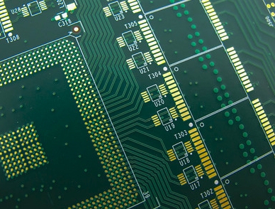
High-density interconnect (HDI) technology for multi layer PCB
High-density interconnect (HDI) technology increases the density and complexity of interconnections within PCBs by integrating more components and circuits into smaller form factors. Micro vias, small diameter holes drilled into the PCB substrate, create connections between circuit board layers. Microvias allow for denser trace and routing, allowing designers to integrate more functionality into a smaller footprint. Additionally, microvias reduce signal propagation delays and improve signal integrity by minimizing signal distortion and impedance mismatch. Create multilayer PCBs with multiple layers of microvias and fine-pitch traces by utilizing advanced manufacturing processes such as laser drilling, sequential build-up (SBU), and thin-film deposition.
The rise of flexible and rigid-flex multi-layer PCB
Rigid-flex multilayer PCBs combine rigid and flexible substrates in a single PCB assembly, allowing for the integration of frozen sections with flexible interconnects. This hybrid structure combines the advantages of rigid and flexible PCBs, including the ability to support high-density interconnects, withstand mechanical stress, and accommodate complex geometries. Industries commonly use rigid-flex boards, such as aerospace, military, and industrial systems, in applications where reliability and durability are critical.
A key benefit of flexible and rigid-flex multi layer PCBs is reducing the need for complex wiring harnesses and connectors, simplifying assembly, reducing weight, and increasing reliability. By integrating multiple layers of circuitry and interconnects into a single flex or rigid-flex PCB, designers can significantly save space and optimize component layout, resulting in more compact and lightweight electronic devices. Additionally, they provide better signal integrity and EMI performance.
Enhanced signal integrity and power distribution
The emerging technology of multi-layer PCB can also reduce signal attenuation and interference, thereby improving signal integrity. Utilizing multiple layers of conductive traces and ground planes provides superior impedance control and reduced signal crosstalk compared to single- or double-layer PCBs. This helps maintain signal integrity by minimizing reflections, distortion, and electromagnetic interference (EMI), ensuring reliable communication between components and minimizing data errors. In addition, they support the implementation of advanced signal routing techniques such as controlled impedance routing, differential signaling, and matched length traces. These techniques help ensure uniform signal propagation and minimize signal deviations, enabling high-speed data transmission while reducing latency and jitter.
Ultimately
Emerging trends and technologies drive innovation and advancement in multi-layer PCBs. Advances in materials science and embedded technology, as well as the rise of flexible and rigid-flex PCBs, allow engineers and manufacturers to unlock new capabilities, achieve higher levels of performance, and meet the ever-changing needs of the electronics industry.