
Exploring the Impact of Copper Foil Thickness Uniformity on Low Loss PCB Performance
Achieving optimal board performance is essential in the PCB world, especially in critical signal integrity applications. Among them, low loss PCB can minimize signal attenuation and distortion and ensure reliable transmission of high-frequency signals. One of the essential factors affecting the performance of low-loss PCB is the uniformity of copper foil thickness. In this technical note, we explore the impact of copper foil thickness uniformity on low loss PCB performance.
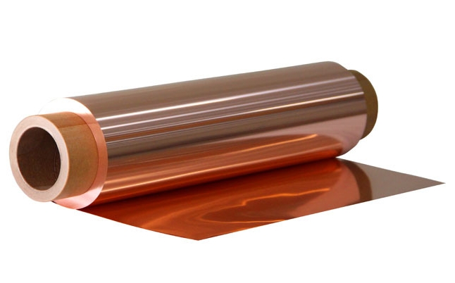
The role of copper foil in low-loss PCB
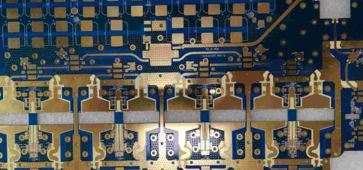
Copper foil is vital in low loss PCBs, especially in facilitating signal transmission in high-frequency applications. Copper’s solid conductivity can facilitate signal transmission on PCBs very well. Its high conductivity ensures minimal resistance, allowing signals to propagate effectively without significant attenuation or loss. In high-frequency applications, signals tend to propagate mainly on the surface of conductors due to the skin effect. The smooth, uniform surface of copper foil provides a consistent and reliable signal transmission path, helping minimize skin effect losses. In low-loss PCBs, it’s critical to maintain precise control over copper foil thickness to reduce signal loss and ensure high signal integrity.
The impact of changes in copper foil thickness on low-loss PCB signal integrity
Copper foil thickness uniformity is vital in minimizing signal loss in low loss PCBs. When the thickness of the copper foil on the PCB surface changes, it can cause impedance mismatch, signal reflection, and attenuation. These changes create discontinuities in the transmission line, resulting in signal loss and distortion. Even minor deviations in copper foil thickness can significantly impact signal integrity, especially in high-frequency applications where impedance control is critical. In addition, changes in copper foil thickness can cause impedance mismatches on transmission lines, resulting in signal reflections and degradation of signal quality. This phenomenon becomes more pronounced at higher frequencies with shorter signal wavelengths.
Method for measuring copper foil thickness uniformity in low loss PCBs
Optical inspection is a standard method of measuring the uniformity of copper foil thickness in low-loss PCBs, where a specialized instrument is used to scan the PCB surface and measure the copper foil thickness at various points. This method provides fast and non-destructive measurements, making it suitable for online quality control. However, the accuracy of optical inspection can be limited, especially for thin copper foils or complex PCB geometries.
Another method involves using a mechanical probe or profilometer to measure the copper foil’s thickness physically. This method provides greater precision and accuracy than optical inspection but may require more time and resources. Advanced techniques such as X-ray fluorescence (XRF) spectroscopy can also be used to analyze the composition and thickness of copper foil non-destructively. XRF spectroscopy provides a detailed understanding of the elemental composition of the foil and can detect thickness changes with high sensitivity.
Optimize copper foil thickness uniformity
First of all, it is fundamental to choose high-quality copper foil materials with precise thickness specifications. Advanced manufacturing techniques are critical to achieving uniform copper foil thickness across the entire low-loss PCB surface. These techniques minimize foil thickness variations due to uneven surface roughness or substrate irregularities. In addition, integrating automated inspection systems into the manufacturing workflow allows for real-time monitoring and feedback on copper foil thickness uniformity. Optical inspection systems or laser-based profilometers can accurately measure foil thickness at multiple points, allowing for timely adjustments and corrective actions.
The Challenge of Achieving Copper Foil Thickness Uniformity
These include the variability inherent in the manufacturing processes involved in production. Factors such as substrate material properties, etching technology, and lamination processes may cause fluctuations in copper foil thickness. Another challenge arises from the complex interaction between copper foil and substrate. Variations in substrate flatness, surface roughness, and dielectric constant can affect copper adhesion and distribution during lamination, resulting in uneven foil thickness. Balancing these factors to achieve optimal adhesion and uniformity is a significant challenge for manufacturers. Additionally, the demand for increasingly thinner and lighter PCBs exacerbates the challenge of attaining uniform copper foil thickness. Thinner foils are more susceptible to manufacturing process variations and may require specialized handling techniques and equipment to maintain consistency.
Improving performance of low-loss PCBs
Copper foil thickness uniformity is critical in determining low-loss PCB performance, especially in high-frequency applications. Variations in copper foil thickness can cause impedance mismatches, signal reflections, and attenuation, compromising signal integrity and reliability. By reading this article, we can learn that using advanced metrology tools and optimized manufacturing processes can ensure the uniformity of copper foil thickness on low-loss PCBs to maximize performance.