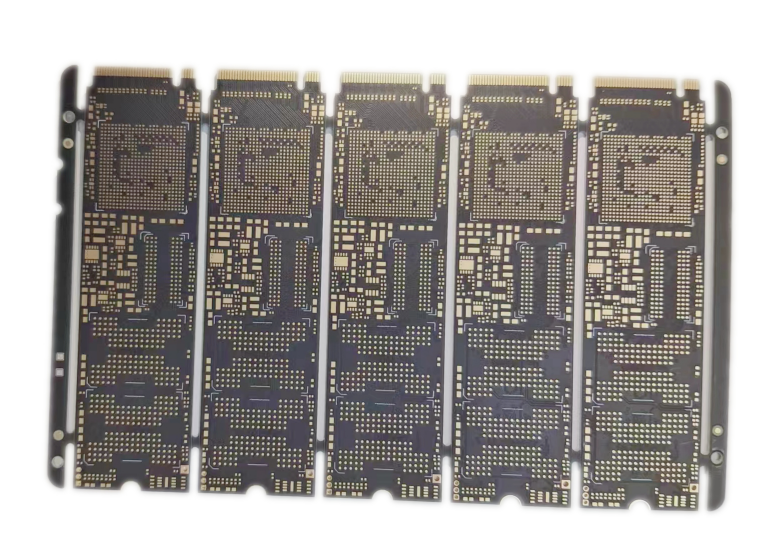
SSD PCB is a type of printed circuit board designed specifically for use in solid-state drives, utilizing advanced materials and technologies to support high-speed data storage. These PCBs are typically used in consumer electronics, enterprise storage systems, and high-performance computing applications. The key benefits of SSD PCBs are their ability to efficiently manage data transfer, integrate flash memory chips, and ensure durability, making them an essential component in modern data storage solutions.
Key Parameters:
Copper Thickness: Typically, copper thickness ranges from 1 ounce to 3 ounces.
Dielectric Material: Typically FR4 or high-frequency laminated insulating copper layer.
Line Width and Distribution: Narrower lines are used for high-speed signals, while wider lines are used for power transmission.
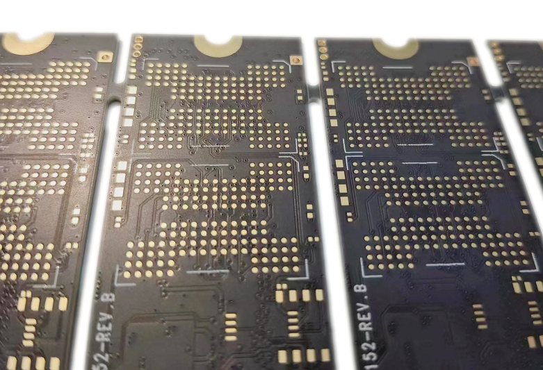
Via Size and Plating: The size of the via and the quality of the copper plating are critical to signal reliability and the overall performance of the SSD.
Thermal Management: PCBs may include thermal vias and deep or embedded copper planes to remove heat generated by memory chips, controllers, and other components.
Surface Finish: Common surface finishes include ENIG (electroless nickel immersion gold), HASL (hot air solder leveling), and OSP (organic solderability preservative).
Impedance Control: PCB design must control the impedance of traces, significantly differential pairs used in data signals, to ensure accurate data transmission without reflections or losses.
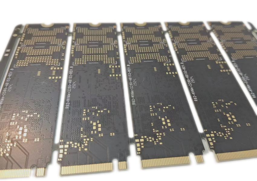
Component Placement and Kitting: The placement of components, including chips, controllers, and connectors, must be optimized for signal routing and power distribution.
Electrical testing and reliability: The PCB undergoes rigorous electrical testing to ensure that all signal, power, and data transfer paths function correctly.
If necessary, you can click to view more of our cases.
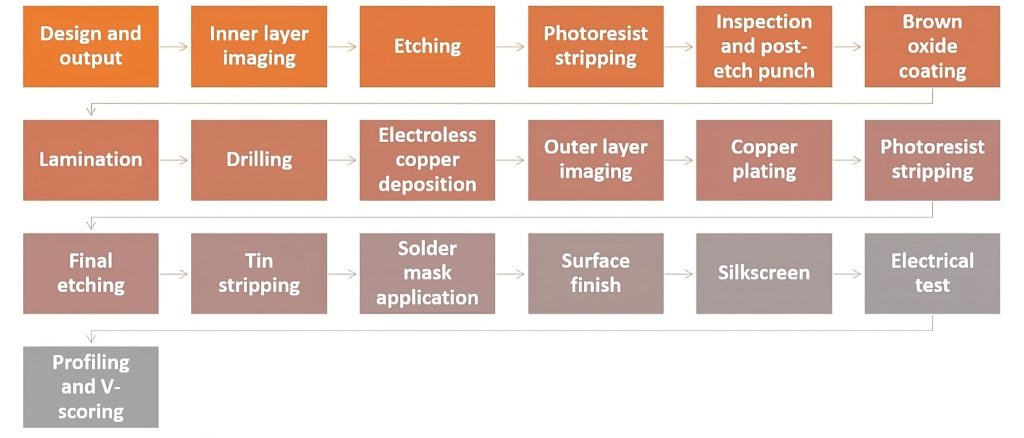
Manufacturing Process:
Layering: The base material is layered with copper foils on both sides, forming the foundation of the PCB.
Circuit Design: The PCB layout ensures proper trace widths and spacing for high-speed data transfer and power delivery.
Laminating: The copper and dielectric layers are bonded under heat and pressure to form a solid PCB.
Drilling: Precision drilling creates holes for vias and components.
Copper Plating: Copper is electroplated to build up the copper traces and vias to the required thickness.
Etching: Excess copper is removed, leaving the designed circuit traces.
Solder Mask Application: A solder mask protects the copper traces and exposes only the areas where components will be soldered.
Silkscreen Printing: Component labels and other markings are printed on the surface of the PCB.
Surface Finish: A surface finish, such as ENIG or HASL, is applied to protect the copper and improve solderability.
Testing and Inspection: The final PCB is tested for electrical integrity and inspected for quality.
Advantages of SSD PCB PCB
✔ Consumer Electronics: Smartphones, tablets, and smartwatches.
✔ Automotive Electronics: Advanced driver-assistance systems (ADAS), sensors, and infotainment.
✔ Medical Devices: Wearable health monitors, imaging systems, and diagnostic tools.
✔ Aerospace & Defense: Satellite systems, avionics, and military-grade equipment.
✔ Telecommunications: 5G base stations, network hardware, and RF devices.
SSD PCB VS. HDD PCB