
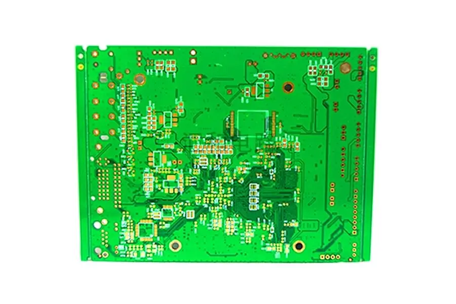
What is a 2 layer TG170 pcb?
We can see various types of PCBs when designing different applications, among which the 2 layer TG170 PCB stands out as a multifunctional and high-performance PCB. We will explore the fundamental aspects of 2-layer TG170 PCBs in this article, clarifying their composition, applications, and advantages in electronic design.
What is a 2 layer TG170 PCB?
2-layer TG170 PCB refers to a PCB characterized by its specific materials and thermal properties. TG, the glass transition temperature, represents the temperature at which the PCB substrate material changes from a rigid state to a more flexible state. TG170 means the glass transition temperature is 170 degrees Celsius.
They are typically made from substrate materials that can withstand higher temperatures, and TG170 ensures that PCBs can withstand high temperatures during manufacturing processes such as soldering and assembly without adverse changes in their physical or electrical properties. A 2-layer configuration means the PCB consists of two conductive layers separated by a dielectric material. These layers allow routing and distribution of electrical signals, with connections allowing signals to travel vertically between them.
2 Layer TG170 PCB Cross-Industry Applications
In automotive electronics, 2-layer TG170 PCBs are often used due to the need to withstand high temperatures. TG170 material ensures that PCBs maintain structural and electrical stability, making them ideal for engine control units, sensors, or in-car entertainment systems. The 2-layer TG170 PCB is also suitable in the industrial sector, providing thermal resilience in extreme temperatures, vibrations, or industrial process environments that generate heat. Products in consumer electronics, including high-performance gadgets and equipment, can benefit from the thermal resilience of TG170 PCBs. From smartphones and tablets to smart home devices, you can improve the lifespan and reliability of consumer electronics.

Advantages of 2 Layer TG170 PCB
There are several advantages to choosing a 2-layer TG170 PCB for your design. Its high thermal reliability ensures the PCB maintains structural and electrical stability even in high-temperature environments. 2-layer configuration combined with TG170 material enhances structural integrity. This is particularly beneficial in applications where the PCB may be subject to mechanical stress, vibration, or other external forces. The thermal stability and rugged construction of TG170 PCB contribute to the longevity and durability of electronic systems.
Manufacturing process
The manufacturing process of a 2-layer TG170 PCB involves several key steps, starting with selecting TG170 grade laminate materials. These materials have a specific glass transition temperature of 170 degrees Celsius, ensuring that PCBs can withstand high temperatures without compromising their structural integrity.
The selected substrate is prepared by cutting it into the desired size and shape, and then a thin layer of copper is deposited onto the substrate through a process called copper pouring. This forms the conductive layer needed to route electrical signals. Next, apply a layer of photoresist material on the copper-clad substrate. The PCB undergoes exposure to ultraviolet (UV) light through a photomask bearing the desired circuit pattern. Developing the exposed photoresist then exposes the copper areas, forming the circuit traces.
The uncovered copper areas are etched away using an appropriate etchant, leaving defined circuit traces. Drilling holes are then drilled into the PCB for component mounting and interconnection. The drilled holes are then plated with conductive material to create electrical connections between the layers. Finally, screen printing prints information such as component labels, reference designators, and logos onto the PCB. The company takes strict quality control measures to ensure compliance with specifications and industry standards.
Design considerations
A 2-story design means a more straightforward structure but requires thoughtful planning. Designers often place ground and power planes on separate layers to minimize interference. Proper layer stacking is critical for signal integrity and impedance control. Trace width and spacing must be consistent with the manufacturer’s manufacturing capabilities to mitigate crosstalk and signal distortion. Pay attention to component placement to reduce signal propagation distance and ensure efficient routing. Also, consider heat dissipation to prevent components from overheating and maintain sufficient clearance to facilitate the assembly process.
Ultimately
We thoroughly explore the 2-layer TG170 PCB from its elemental composition to its diverse applications and manufacturing considerations. Ensure that more users and designers can understand it more intuitively.