
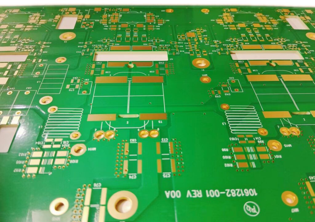
Improve application performance and reliability with 2 layer heavy copper pcb
Performance and reliability are crucial in electronic applications, and the factors that affect these two aspects mainly focus on PCB. In this article, we will introduce how 2 layer heavy copper pcb can improve the functionality of various electronic devices and systems, from enhanced power distribution to improved thermal management and more.
The role of 2 layer heavy copper pcb
It is often required to provide reliable power connections to electronic devices, whose primary function is to provide a current path with low resistance and high conductivity. Copper is known for its excellent electrical conductivity, and 2 layer heavy copper PCB reduces electrical resistance. This is critical for power connections in electronics, where minimizing resistance is essential to prevent voltage drops and ensure efficient power transfer. Lower resistance means less heat loss, allowing more energy to reach its intended destination within the electronic device.
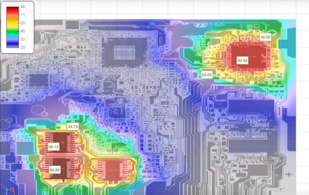
2 layer heavy copper PCB optimized thermal management
Thermal challenges are common problems in electronic applications. In the area of optimizing thermal management, the thickness of a 2 layer heavy copper PCB is a critical factor in thermal management. Thicker copper layers have better thermal conductivity and can effectively dissipate the heat generated during the operation of electronic components. Its thermal resistance is significantly reduced, allowing for more efficient heat dissipation, preventing local overheating, and maintaining a more stable operating temperature for the entire electronic system. Additionally, its layered structure enables the integration of additional thermal management features. Heat sinks or thermal vias can be strategically placed on the PCB to facilitate heat dissipation further.
Powering high-frequency applications
High-frequency applications often involve fast signal transitions and require low impedance to maintain signal integrity. The lower resistance of the 2-layer thick copper PCB minimizes signal loss, ensuring that high-frequency signals reach their destination with minimal attenuation. At the same time, copper’s enhanced thermal conductivity further supports the efficient dissipation of heat generated during high-frequency operation. This is especially important for applications where components experience fast switching and high power densities. The thick copper layer acts as an efficient thermal conductor, preventing local overheating and ensuring the stability of electronic components. High-frequency signals are sensitive to changes in impedance, and a 2-layer thick copper PCB design facilitates precise impedance control.

Reduce signal loss for reliable connections
Efficient power transfer is another advantage offered by 2 layer heavy copper pcbs. In applications that require large amounts of current or power distribution, it can reduce voltage drop, ensuring that the intended power reaches its destination without significant losses. This is especially important in power-sensitive applications where a reliable power connection is critical for optimal device performance. Additionally, its layered structure enables efficient ground plane implementation. A dedicated ground plane helps minimize electromagnetic interference (EMI) and crosstalk between traces, enhancing signal reliability.
Strength of 2 layer heavy copper PCB
In high-stress environments, the reliability of electronic systems is critical, and 2 layer heavy copper PCB printed circuits The ruggedness and mechanical strength of 2 layer heavy copper PCB PCB configurations can withstand physical stress, vibration, and harsh conditions to ensure the long-term longevity of electronic equipment stability. Thicker copper layers increase the overall rigidity of the PCB, making it more resistant to bending, flexing, and external forces. This is especially important in applications where the PCB may be subject to mechanical stress or vibration. Its layered structure provides additional support to withstand mechanical stress. The sandwich design enhances the overall structural integrity of the circuit board and reduces the risk of warping or deformation when exposed to external forces. This feature ensures it remains intact in challenging conditions.
Improve electronic performance
From efficient power distribution and thermal management to signal integrity, it can become a PCB with enhanced electronic capabilities, ideal for lighting applications and telecommunications equipment. With the development of technology, more and more people are incorporating 2-layer thick copper PCB into electronic designs.