
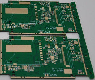
Customization Options for 2 Layer TG150 PCB Designs
When designing PCBs, a customized approach can be used to meet the specific requirements of different users. Therefore, in this section, we will introduce the available customization options when customizing a 2 Layer TG150 PCB, emphasizing the importance of flexibility in meeting different application requirements.
Choosing the suitable substrate for your 2 layer TG150 PCB
When customizing, the first thing to consider is the different material options. For 2 layer TG150 PCB there are usually high Tg FR-4, ITEQ IT-180A, Isola 370HR, Nelco N4000-13EP, Rogers RO4350B, and other options. When we select a substrate, we need to consider factors such as dielectric constant (Dk) and dissipation factor (Df). Low Dk ensures signal integrity, while low Df minimizes signal loss. Substrate thickness is critical, affecting impedance control and mechanical strength.
layout design
Customization options for its layout design include adjusting the location of different key components to reduce signal interference, enhance power distribution, and effectively manage thermal dissipation. Custom signal paths also allow engineers to optimize trace lengths, widths, and configurations to meet specific impedance requirements, reduce signal distortion, and improve overall performance. Custom solder mask and screen printing options provide aesthetic and functional choices. Different colors and markings aid in assembly and troubleshooting, providing a visual guide for technicians handling PCBs.
2 Layer TG150 PCB Customized Special Components
First, selecting specialized components that match the intended functionality is crucial. These can include sensors, ICs, or other devices customized to the application’s needs. Custom packaging of these specific components ensures seamless mounting onto a 2 Layer TG150 PCB. Engineers customize the size and shape of pads and holes to match the specifications of the integrated components, promoting efficient soldering and mechanical stability. Among them, power distribution customization is crucial for stable functionality. Engineers customize the layout to effectively manage power flow, prevent problems such as voltage drops, and ensure consistent power to integrated components.
Design for Manufacturability (DFM)
Design for manufacturability (DFM) is crucial in balancing customization and production feasibility. DFM focuses on optimizing designs to make manufacturing processes more efficient and cost-effective. Balancing customization with DFM involves careful component placement. Engineers must optimize the layout to minimize production challenges and ensure components can be installed and welded efficiently during manufacturing. At the same time, the packaging of custom components must comply with DFM principles to achieve a balance between efficient manufacturing processes.
Use customization to define your PCB
In the article, we told you about the countless customization options for the 2-layer TG150 PCB design. From material selection to layout accuracy and the integration of advanced technologies, as designers face the complexity of electronic applications, the ability to customize 2-layer TG150 PCBs to specific needs ensures that electronic products meet the needs for innovation and reliability.