
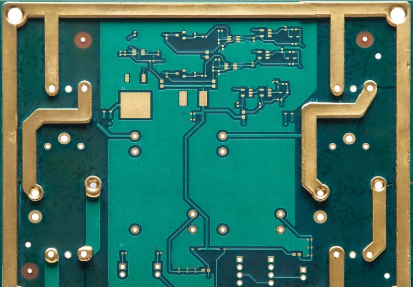
Effect of Copper Particles on Heavy Copper PCB
The electrical performance of heavy copper PCB can be affected by various factors, including the structure of the copper particles used in manufacturing. Copper particle structure refers to the arrangement and shape of copper particles within the PCB substrate. In this guide, we look closer at the importance of copper particle structure and its impact on the electrical performance of heavy copper PCBs.
The role of copper particle structure in the conductivity of heavy copper PCBs
Its lattice structure and grain boundaries mainly determine the conductivity of copper in heavy copper PCB. Copper particles are arranged in a lattice structure to form crystal grains. The size of copper particles in the lattice structure will directly affect the conductivity of heavy copper PCB. Smaller grain size results in fewer grain boundaries and less electron scattering, resulting in higher electrical conductivity. Conversely, larger grain sizes increase the number of grain boundaries, impeding electron flow and reducing electrical conductivity. Certain crystal orientations provide lower resistance paths for electron flow, resulting in higher conductivity in specific directions within the material. Aligning copper grains during manufacturing can enhance the conductivity of thick copper PCBs.
Effect of Copper Particle Structure on Signal Integrity of Heavy Copper PCBs
The structure of copper particles plays a vital role in determining signal integrity, which refers to the reliability and quality of electrical signals transmitted through a PCB. First, the grain size of the copper particles affects the conductivity of the trace. Smaller grain sizes provide more grain boundaries, impeding electron flow and increasing resistance, causing signal attenuation and loss. Therefore, larger grain sizes are preferred for high-conductivity traces to minimize signal attenuation. Secondly, the orientation of copper particles affects the PCB’s mechanical and electrical properties. The aligned grain structure allows for better electron flow along the traces, reducing signal distortion and increasing transmission efficiency.
Thermal Management and Copper Particle Structure
The structure of copper particles directly affects PCB’s thermal conductivity and heat dissipation capabilities. Copper is an excellent thermal conductor and can efficiently transfer thermal energy from heating components to a heat sink or other cooling mechanism. Then, the arrangement and size of the copper particles also affect the overall thermal performance of the PCB. The particle size of copper particles affects thermal conductivity. Larger grain sizes reduce the number of grain boundaries and allow heat to flow more freely through the material, providing better thermal conductivity. Second, the distribution of copper particles on the PCB surface affects thermal uniformity. Therefore, properly dispersed copper particles promote effective heat dissipation throughout the PCB, thus aiding in effective thermal management.
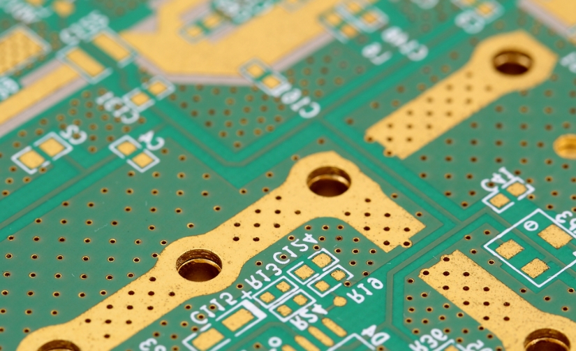
Copper particle structure and plating adhesion
In the manufacturing of thick copper PCB, the copper particle structure and electroplating adhesion are important factors affecting the reliability and performance of heavy copper PCB. First, the copper particle structure refers to the arrangement of copper particles within the PCB copper layer. In thick copper PCBs, we typically deposit the copper layer through processes such as electroplating or lamination. Layers can significantly affect the mechanical and electrical properties of a PCB. Plating adhesion on thick copper PCB refers to the bonding strength between the copper layer and the plated surface. Adequate plating adhesion is critical to prevent delamination or peeling of the copper layer during manufacturing or handling, which can compromise the structural integrity and functionality of the PCB.
Several factors can affect plating adhesion, including surface preparation, cleanliness, and the quality of the copper particle structure. Appropriate use of some surface treatments can promote mechanical interlocking between the copper layer and the electroplated surface, thereby enhancing the bonding strength.
Optimizing Copper Particle Structure for Thick Copper PCBs to Improve Electrical Performance
How can we optimize the copper particle structure of thick copper PCBs to enhance electrical performance? The priority is to control the grain size of copper particles, and optimizing the grain size within the appropriate range is crucial to balance electrical conductivity and mechanical strength. The second step is to ensure that we evenly distribute the copper particles on the PCB surface, which promotes consistent conductivity and impedance characteristics. Uneven distribution or aggregation of copper particles can cause localized changes in electrical properties, resulting in signal distortion and impedance mismatch. We can improve electrical performance by aligning copper particles along the direction of current flow to reduce electron scattering and enhance conductivity.
In general
The structure of copper particles in heavy copper PCB determines its electrical performance. By understanding the impact of copper particle structure on conductivity, signal integrity, thermal management, etc., the design and manufacturing process can be optimized to meet the stringent requirements of various applications.