
The impact of gold finger pcb on EMI/RFI shielding
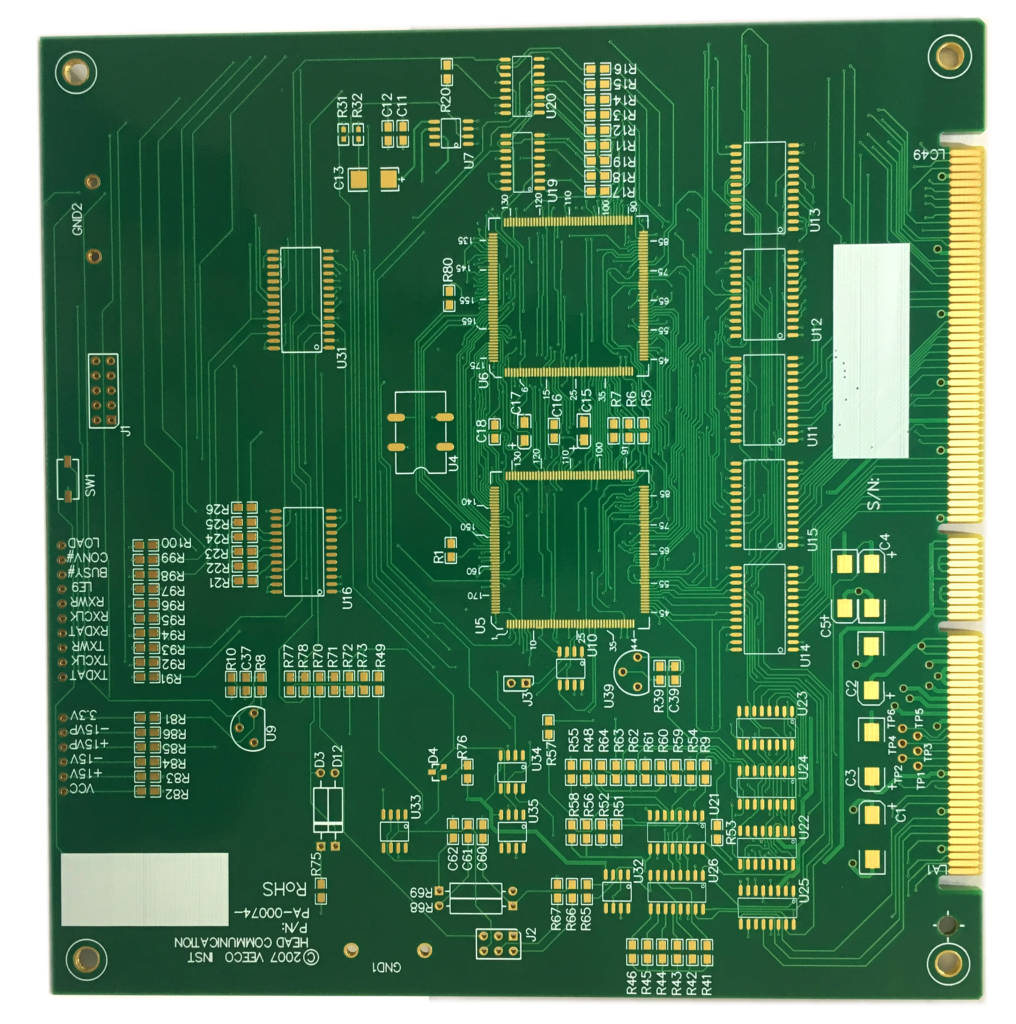
Their gold-plated edge connectors characterize gold finger PCB. In addition to their primary function of facilitating electrical connections, Gold finger PCBs also provide significant advantages in electromagnetic interference (EMI) and radio frequency interference (RFI) shielding. In this guide, we explore the impact of gold finger PCBs on EMI/RFI shielding, illustrating how gold finger PCBs can help mitigate electromagnetic interference and ensure optimal performance in electronic applications.
The Basics of EMI/RFI Shielding and Why It’s Important
Electromagnetic interference (EMI) and radio frequency interference (RFI) are harmful electromagnetic signals that can disrupt the proper operation of electronic devices and systems. EMI and RFI can disturb the proper functioning of electronic equipment, causing signal attenuation, data corruption, and even equipment failure or failure. Shielding involves using materials and techniques to contain these electromagnetic emissions and prevent them from interfering with sensitive components or nearby electronic equipment. Effective EMI/RFI shielding is essential to maintaining signal integrity and minimizing electromagnetic contamination. The importance of shielding against EMI/RFI cannot be overstated, especially in industries such as telecommunications, aerospace, automotive, and medical, where reliable operation is critical. Performance degradation, increased susceptibility to interference, and shortened service life may occur without proper shielding.
Unique Properties of Gold Finger PCB for EMI/RFI Shielding
Gold finger PCBs, known as gold-plated edge connectors, exhibit unique EMI/RFI shielding capabilities. They can transmit signals efficiently and minimize signal loss. This high conductivity helps maintain signal integrity and reduce electromagnetic interference. In addition, gold is highly resistant to corrosion, ensuring the long-term reliability and durability of Gold finger PCBs. Gold-plated contact pads provide low contact resistance, ensuring a reliable electrical connection and minimizing signal degradation. This low resistance helps optimize signal transmission and reduces the risk of electrical noise or interference.
Effect of Gold Plating Thickness on EMI/RFI Shielding Performance
The gold plating thickness on the gold finger PCB can directly affect the PCB’s electromagnetic interference (EMI) and radio frequency interference (RFI) shielding performance. It determines the PCB’s anti-interference ability in the electromagnetic environment. Typically, the thicker the gold plating on a gold finger, the better its conductivity and shielding effect. Increasing the gold plating thickness of gold fingers can effectively reduce the interaction between the PCB and electromagnetic interference in the external environment. Metal layers achieve this shielding effect through reflection and absorption. A thicker gold-plated layer can provide a better shielding effect and reduce the propagation and interference of electromagnetic waves.
Enhance EMI/RFI shielding through correct gold finger PCB design and layout
The shielding effect of EMI/RFI can also be enhanced through proper gold finger PCB design and layout. Gold fingers are gold-plated contact points on the PCB and play a key role in minimizing EMI/RFI interference. When designing gold finger PCBs, a strategic layout ensures proper spacing between gold fingers and other components, which helps reduce signal crosstalk and interference. In addition, EMI/RFI protection is further enhanced with a ground plane and shielded housing. Additionally, controlled impedance cabling and proper grounding can improve EMI/RFI protection by reducing signal reflections and improving overall signal integrity.
Common challenges and considerations for shielding EMI/RFI gold finger PCB
When using gold finger PCB to shield EMI/RFI, the challenge lies in selecting the appropriate materials for the PCB substrate and gold finger contacts. Using high conductivity and low impedance materials helps minimize signal loss and interference. Ensuring proper grounding is another critical consideration. Effective grounding techniques help dissipate electromagnetic energy and reduce the risk of ground loops, which can introduce unwanted noise. Additionally, it is essential to consider the manufacturing process. Ensuring uniform gold finger plating thickness and controlling solder joint quality is critical to achieving consistent EMI/RFI shielding performance.
Ultimately
Gold finger PCBs offer significant advantages for EMI/RFI shielding applications due to their unique features and design. By utilizing gold plating thickness and Gold Finger PCB design and layout techniques, designers can maximize the shielding effectiveness of Gold Finger PCBs and ensure optimal performance of electronic devices and systems.