
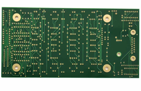
How does 2 layer TG170 PCB improve the performance of electronic devices?
Improving performance and efficiency is vital in today’s rapidly developing electronics industry. Therefore, engineers and designers are constantly looking for solutions to enhance the functionality of their electronic devices. One of the solutions is to use a 2 layer TG170 PCB, and in this comprehensive guide, we’ll explore tips and strategies for optimizing performance using a 2-layer TG170 PCB. From design considerations to manufacturing techniques, we’ll delve into every aspect to help users and consumers unlock the full potential of their electronic devices.
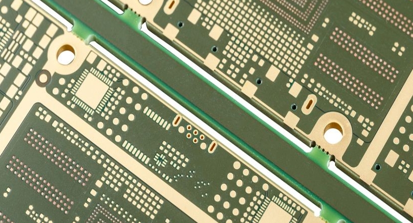
2 layer TG170 PCB layout and routing reduces signal loss and crosstalk
First, careful component placement is crucial. Strategically and compactly placing components minimizes the distance between components and reduces the length of signal traces. This shorter path reduces signal propagation delay and attenuates signal losses along the transmission line. They can mitigate crosstalk through properly spaced wiring. Maintaining sufficient distance between signal traces and avoiding them crossing at right angles can significantly reduce the risk of crosstalk. In addition, the use of differential signaling techniques and controlled impedance circuits can also mitigate signal crosstalk and ensure reliable communication between components.
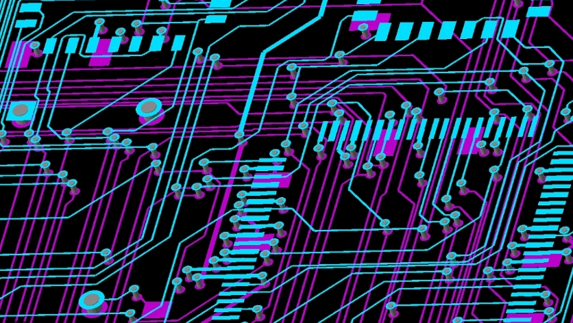
2-layer TG170 PCB solves electronic device signal integrity challenges
2 layer TG170 PCBs typically feature thicker copper layers and improved dielectric properties, which help minimize electronic device signal loss and impedance mismatches. They place signal traces on the outer layer and place the ground or power plane on the inner layer to enhance signal integrity. Reducing signal discontinuities with proper routing techniques can help minimize signal reflections and impedance changes, and routing differential pairs with equal lengths and spacing can minimize timing skew and ensure signal synchronization.
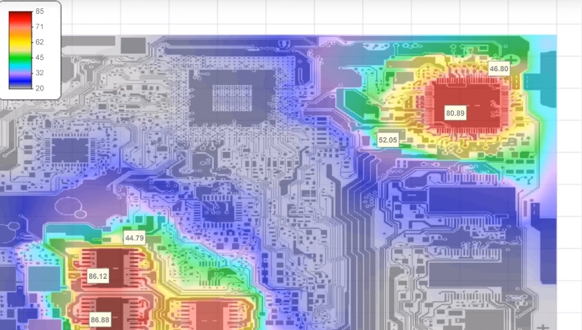
Thermal Management Strategies for 2 Layer TG170 PCB
They use thermal pads and vias to efficiently transfer heat from thermal components to the ground or power planes of a 2 layer TG170 PCB. Thermal vias provide a low-impedance path for heat dissipation, while thermal pads increase thermal conductivity between the component and the PCB substrate. Thermal traces are also incorporated into the design of the 2 layer TG170 PCB, which reduces the thermal resistance between the element and the PCB copper layer, thereby increasing thermal conductivity and reducing the risk of overheating high-power components.
It can also help to enhance cooling by attaching a heat sink or thermal pad to high-power components. This allows the heat sink to increase the heat transfer surface area while the thermal pad provides a direct thermal interface between the element and the heat sink or PCB. Their materials also have enhanced thermal properties, ensuring stable performance in high-temperature conditions.
Mechanical strength and durability
2-layer TG170 PCB provides excellent mechanical strength and durability, especially in harsh environments. Its high TG ensures stability even at high temperatures, preventing deformation or softening during operation, thereby increasing overall mechanical strength. Secondly, the double-layer copper foil structure enhances mechanical support. Copper foil facilitates good electrical connections and withstands mechanical stress and impact, ensuring durability. Whether deployed in automotive systems, industrial machinery, or consumer electronics, 2 layer TG170 PCBs provide unparalleled reliability and durability, guaranteeing long-term stable performance.
High-frequency performance
They provide impressive high-frequency performance, supporting advanced technologies in various electronic applications. They are made of low dielectric loss materials, allowing signals to propagate with minimal attenuation even at high frequencies. This ensures accurate and reliable transmission of high-frequency signals. Their precise impedance control is critical to maintaining signal integrity in high-frequency circuits. They are designed with proper spacing and isolation techniques to minimize crosstalk and maintain signal integrity for the application.
Significantly improve the performance of electronic equipment
The many advantages of 2-layer TG170 PCB greatly enhance the performance of electronic devices. From superior thermal management and improved signal integrity to mechanical strength and durability, they are the first choice for designers and engineers looking to optimize electronic designs. By leveraging the unique properties of 2-layer TG170 PCBs, users, and consumers can unlock new possibilities in electronic device design.