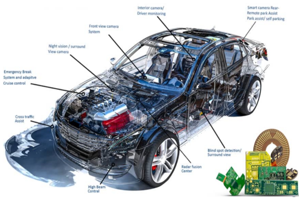
Heavy copper PCB, also known as thick copper PCB, is a printed circuit board with a much thicker copper layer than a standard PCB. These boards are designed to handle high currents and dissipate heat efficiently. Thick copper PCBs are designed to handle high current levels, making them suitable for applications in power electronics, high-voltage circuits, and high-current components.
Key Parameters:
Copper Thickness: Heavy copper PCBs are defined by their thick copper layers. These can range from 2 ounces (2oz) up to 20oz or more, with 3oz and 6oz being common for power applications.
Copper Weight Distribution: The distribution of copper weight across the board is essential for managing current-carrying capacity. This includes the thickness of the traces and the plane areas.
Thermal Management: Heavy copper PCBs often include additional features like thermal vias or heat sinks to manage and dissipate heat effectively.
Dielectric Thickness: The thickness of the insulating dielectric material between copper layers is crucial to prevent short circuits.
Trace Width and Spacing: Proper trace width and spacing are necessary to handle high currents without overheating or electrical issues.
Hole Size and Plating: The hole size and the quality of copper plating in vias are essential to ensure electrical connections between layers.
Surface Finish: The choice of surface finish depends on the specific requirements of the PCB, such as solderability and corrosion resistance.
Design for Reliability: The overall design and layout of the PCB must ensure reliability and robust performance under high-current conditions.
Manufacturing Process:
Layering: The chosen material is layered with copper foils. Typically, heavy copper PCBs have copper layers on both sides of the board, which can be pretty thick.
Circuit Design: The PCB layout and design are critical to ensure that the heavy copper traces carry the required current without overheating. Adequate spacing and trace widths must be considered to prevent short circuits and ensure reliable connections.
Laminating: The layered material is laminated under heat and pressure to create a solid board.
Drilling: Precision drilling is done to create holes for components and vias.
Copper Plating: The heavy copper layers are electroplated to increase their thickness. This is a critical step in manufacturing as it defines the copper thickness, a key parameter for heavy copper PCBs.
Etching: Excess copper is etched away to reveal the copper traces and pads according to the PCB design.
Solder Mask Application: A solder mask is applied to insulate and protect the copper traces while exposing the necessary areas for soldering components.
Silkscreen Printing: Component labels, indicators, and other markings are applied.
Surface Finish: The PCB may receive a surface finish like ENIG (Electroless Nickel Immersion Gold) or HASL (Hot Air Solder Leveling) to improve solderability and protect exposed copper.