
Benefits of Using 4 layer PCB in Electronic Devices
Multi-layer PCB plays a vital role in many applications. In this article, we will introduce the role of 4 layer PCB in modern electronic products, including enhanced functions to improve signal integrity. Each Layer adds a new dimension to the performance and reliability of our favorite devices.
Increase flexibility in electronics with 4-layer PCBs
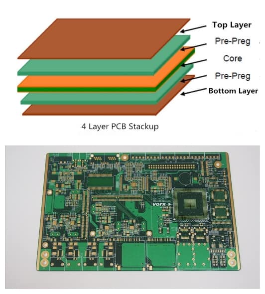
The transition from traditional 2-layer PCBs to 4-layer PCBs has increased the complexity and functionality of electronic designs. Additional layers provide more routing options, allowing engineers to design complex circuits that improve signal integrity, reduce electromagnetic interference (EMI), and enhance thermal management. The first two layers of a 4-layer PCB typically handle the central routing, power distribution, and component placement. This separation of power and ground planes reduces signal crosstalk and improves overall signal integrity. Layers 3 and 4 provide additional routing options, allowing for more complex and compact designs. Additionally, using 4-layer PCBs supports the implementation of mixed-signal designs where analog and digital components coexist.
4-layer PCB enhances signal integrity
A 4-layer PCB usually consists of two signal layers and two plane layers, each with a ground layer and a power layer. This layered structure effectively manages signal trajectories, minimizing signal distortion and enhancing communication reliability. Separating power and ground planes helps reduce noise and interference and provides a more stable environment for signal propagation. The use of additional ground planes helps improve EMI shielding. These features are handy in applications where reliable and high-speed communications are critical, such as data-intensive equipment, network equipment, and high-frequency applications.

Efficient energy management with 4-layer PCB
In a 4-layer PCB, the additional layers beyond the traditional double-sided PCB provide opportunities for more complex power plane layouts. Separating power and ground planes helps minimize impedance and reduce voltage drops, ensuring stable, efficient power delivery to various components within the electronic system. Their dedicated power planes are optimized for power distribution to meet specific power requirements, such as high-current components or sensitive analog circuits. By strategically allocating power planes, designers can minimize interference, reduce crosstalk, and maintain a clean and stable power supply that helps improve energy efficiency.
Meet the needs of modern electronic products
Modern electronic products have stringent requirements for high-speed performance, and 4-layer PC can control impedance design. This involves carefully managing the electrical characteristics of signal traces, such as width, spacing, and layer stacking, to ensure optimal impedance matching. Controlled impedance is essential to prevent signal distortion reflections and maintain the integrity of high-speed data transmission. This makes 4-layer PCBs ideal for data communications, networking, and high-frequency equipment applications. Additionally, the layered structure enables efficient thermal management, a key consideration in high-performance electronics.

Reliability and durability
Reliability and durability are also the most critical considerations in electronic design. The layered architecture of the 4-layer PCB and its specific design features ensure that electronic devices can maintain long-term performance. Separation of power and ground planes within them. This design strategy minimizes noise and interference and provides a stable environment for electronic components. By reducing the possibility of signal crosstalk and interference, 4-layer PCBs help improve the overall reliability of signal transmission.
Finally
The benefits of using 4-layer PCBs in electronic devices extend far beyond the surface. Electronic device performance is greatly improved from enhanced design flexibility to optimized power distribution and enhanced signal integrity. As electronic devices become an integral part of our daily lives, adopting 4-layer PCBs is essential.