
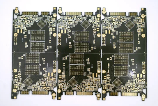
Importance of thermal via layout in 6 layer SSD pcb
Thermal management is critical when designing 6 layer SSD PCBs to ensure optimal performance and reliability. In a high-performance 6 layer SSD PCB, components such as controllers, memory chips, and power regulators generate heat during operation. Excessive heat accumulation can degrade component performance, shorten service life, and cause system failure without effective heat dissipation. Therefore, thermal vias are vital in dissipating heat from sensitive components and maintaining optimal operating temperatures.
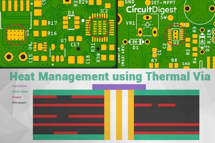
The role of thermal vias in 6-layer SSD PCB in heat dissipation
Thermal vias in the 6 layer SSD PCB play a vital role in dissipating heat, and the 6-layer SSD PCB generates heat during operation due to the current flowing through the components. Over time, excessive heat buildup can reduce SSD performance and reliability, leading to potential data loss or device failure. The multi-layer design of the 6 layer SSD PCB allows thermal vias to be placed at specific locations. When heat is generated, the heat spreads through the vias to the outer layer of the PCB and is dissipated into the surrounding environment through thermal conduction, convection, and radiation.
6 layer SSD PCB thermal via layout for effective heat dissipation
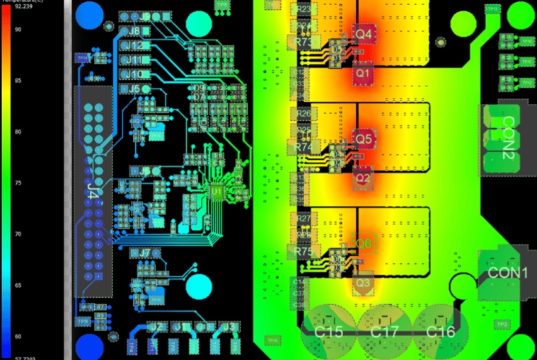
First, when optimizing the thermal via layout, the location of heat-generating components on the 6 layer SSD PCB must be considered. Thermal vias should be strategically placed near these components to provide a direct path for transferring heat away from them. Secondly, the density and distribution of thermal vias should be optimized to ensure uniform heat dissipation across the entire PCB. By evenly spacing thermal vias and placing them in key areas where heat concentration is highest, heat can be dispersed and dissipated more efficiently. In addition, the size and diameter of the thermal vias should be carefully selected. Larger diameter vias provide lower thermal resistance and can carry more heat. Conversely, smaller diameter vias may have higher thermal resistance and require less space.
Solve thermal issues with 6 layer SSD PCB pitch and aspect ratio
The spacing between 6 layer SSD PCB layers is vital in thermal management. The wider spacing between layers allows for better airflow and heat convection, which promotes heat transfer away from the heating components. It also reduces the risk of thermal conduction between adjacent layers, minimizing thermal coupling and preventing local hot spots.
On the other hand, reducing the interlayer spacing can increase the thermal conductivity and enhance heat transfer efficiency. Tighter stacking increases the distance between heating elements and thermal vias, lowering thermal resistance and improving thermal performance. In addition, optimizing the aspect ratio of the PCB layer, especially the width-to-length ratio, can further enhance heat dissipation capabilities. A higher aspect ratio provides a greater surface area for heat transfer, promoting more efficient heat dissipation on the PCB.
Overcoming Thermal Via Layout Design Challenges
One of the significant challenges in thermal via layout design is balancing the need for efficient heat dissipation with maintaining signal integrity. Thermal vias can cause impedance mismatches and signal reflections that can degrade the performance of high-speed data signals. Therefore, we must carefully optimize the placement and distribution of thermal vias to minimize their impact on signal integrity while maximizing heat transfer efficiency. Additionally, ensuring uniform heat distribution is another challenge in thermal via layout design. Variations in component density, power dissipation, and thermal conductivity can cause uneven heat distribution, creating localized hot spots and thermal stresses. Therefore, thermal vias must be carefully distributed and positioned to promote even heat dissipation.
Thermal Via Layout Impact on Reliability and Performance
The placement and distribution of heat dissipation holes directly affect the thermal management capabilities of the 6 layer SSD PCB. Well-distributed thermal vents help effectively transfer heat away from critical components, preventing heat build-up and reducing the risk of overheating-related failure. In addition, the design of the heat dissipation holes also affects their mechanical stability and reliability. Overuse or improper placement of thermal vias can weaken the structural integrity of the PCB, leading to mechanical stress and potential reliability issues such as solder joint fatigue or mechanical failure. Designers must carefully balance thermal management needs with PCB mechanical requirements to ensure long-term reliability and durability.
Effective thermal via layout for enhanced performance
The importance of thermal via layout cannot be ignored. Effective cooling is critical to maintaining optimal performance, reliability, and longevity of high-performance SSDs. Designers can ensure efficient heat transfer by strategically designing and optimizing thermal via layout to improve overall SSD performance.