
What are the considerations when designing a 6 layer SSD pcb?
Because the 6 layer SSD pcb has many layers, we need reasonable control over the design details. This chapter will introduce what designers need to consider when making high-performance, efficient 6-layer SSD PCBs.
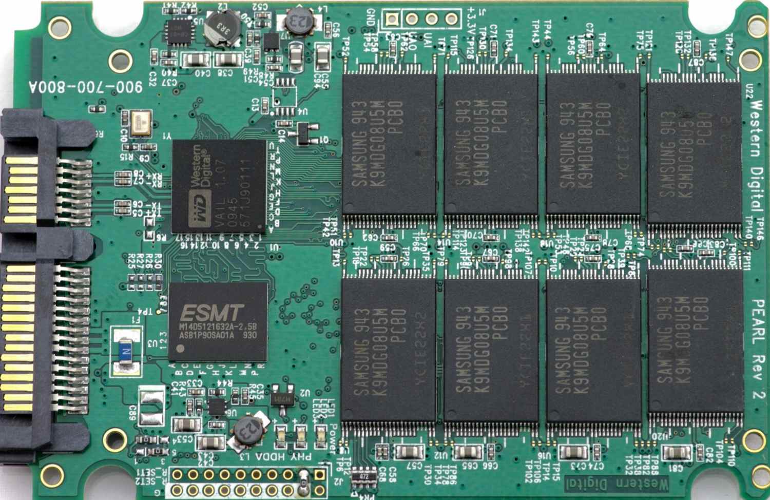
Choosing the suitable substrate when designing a 6 layer SSD pcb
Choosing the right materials to design this PCB is crucial. The substrate material will affect the electrical and thermal performance of the PCB. For this kind of PCB, choosing materials with low dielectric constant and controllable impedance can ensure effective signal transmission and reduce the risk of signal distortion. Layer stacking design is another consideration, requiring careful planning of the layer arrangement to accommodate various components and signal routing. Customized layer stacking allows for optimal signal integrity, power distribution, and efficient thermal management, helping to improve the overall reliability of the SSD.
Ensure robust signal path in 6 layer SSD pcb
When designing, ensure the integrity of their signals. Customizing the trace width, spacing, and layer stacking according to the 6-layer SSD PCB design requirements can help maintain consistent impedance throughout the signal path. This way, reducing signal reflections and distortion ensures that the transmitted data remains accurate and reliable. In addition, our engineers need to focus on customizing layouts and designing vias to connect signal layers during design to minimize signal crosstalk, electromagnetic interference (EMI), and radio frequency interference (RFI). Ensure smooth signal transition between layers.
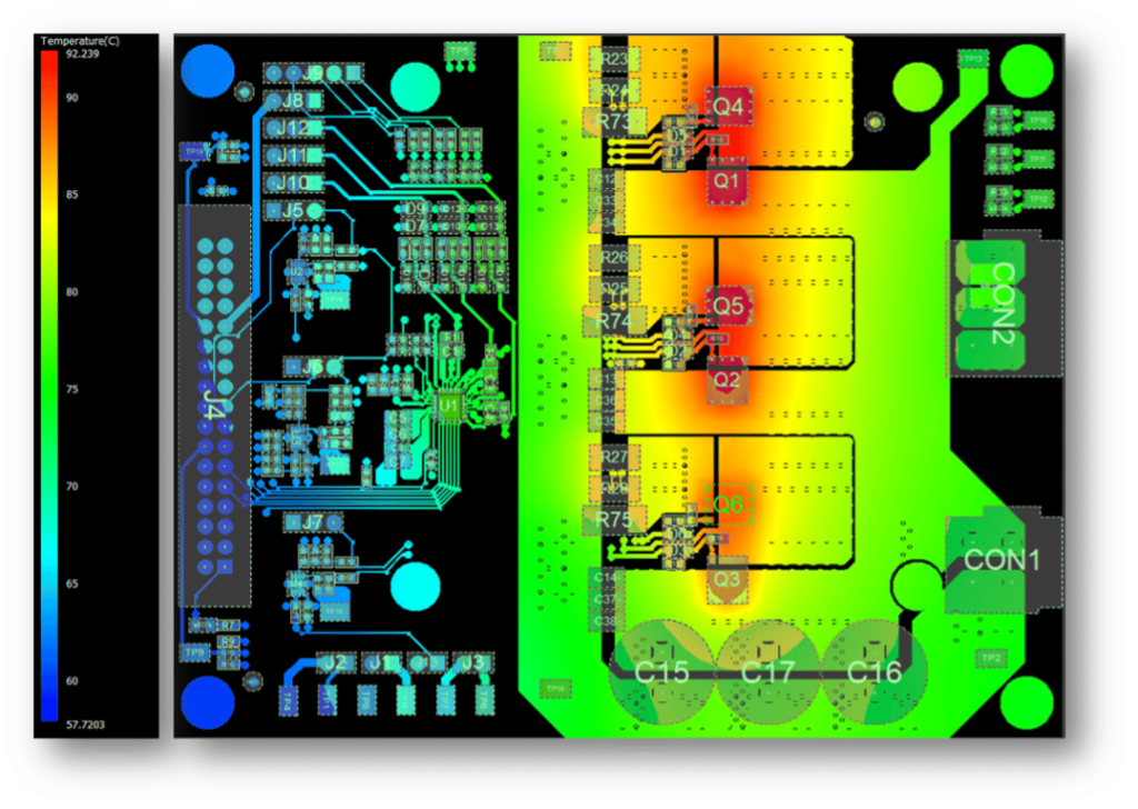
Overcoming Thermal Challenges of 6 layer SSD pcb Design
To overcome thermal challenges in 6-layer SSD PCB design, effective thermal management can be achieved through custom layer stacking design. Optimize heat dissipation by placing power-hungry components and critical heat-generating elements on specific layers. Designers can customize the use of heat sinks and thermal pads for specific 6-layer SSD PCB assemblies. Design engineers can strategically place and design these components to enhance heat dissipation. Custom heat sink and thermal pad sizes, shapes, and materials ensure optimal thermal conductivity and efficient heat transfer.
Integrate advanced design elements
Designers can incorporate NAND flash memory chips for efficient data storage and retrieval during the design process. This reduces signal interference, optimizes data transfer rates, and promotes efficient error correction mechanisms. We can also use advanced components to control the flow of data within the SSD, reducing latency and enhancing the overall performance of the SSD. Proximity to the memory chip and optimized trace routing facilitate efficient data processing. Finally, advanced voltage regulators, capacitors, and inductors can ensure a stable power supply, minimize voltage fluctuations, and improve system reliability.
Manufacturing harmonious design
Standardized component packaging helps harmonize its design and manufacturing. Customizing components to conform to industry standard sizes and shapes facilitates compatibility with automated assembly equipment, reducing production complexity and cost. This standardization ensures seamless integration of advanced elements in the manufacturing process. Coordinated power distribution customization can optimize the layout to reduce power losses and voltage fluctuations. Engineers balance power transmission requirements with manufacturing feasibility to ensure stable operation without compromising manufacturing efficiency.
Ensure performance integrity
From material selection to signal integrity and the integration of advanced technologies, designing them requires a holistic approach to ensure performance integrity. We hope to guide designers through this article to achieve the best possible design.