
Can mid low loss PCB help reduce electromagnetic interference (EMI)?
Electromagnetic interference can destroy the signal integrity of electronic equipment, cause malfunctions, and even cause equipment failure. To solve this problem better, we use mid low loss PCB to reduce EMI effectively. It has significant advantages in reducing EMI and improving overall electronic performance. You can read this article to learn how low to mid low loss PCB can reduce electromagnetic interference and ensure the reliable operation of electronic applications.
Understanding EMI in Electronic Systems
Electromagnetic interference (EMI) is a common phenomenon in electronic systems characterized by the inadvertent generation, transmission, or reception of electromagnetic energy that disrupts the normal operation of electronic equipment. They can manifest in various forms, including electromagnetic radiation, conducted noise, and transient interference. They can occur over a wide frequency spectrum from a few kilohertz to several gigahertz. EMI can originate from internal and external sources, including switching circuits, power supplies, RF transmitters, and environmental factors such as lightning and radio transmissions.

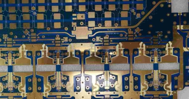
The role of mid low loss PCB in reducing EMI
A key advantage of mid-low loss PCBs in reducing EMI is their ability to maintain signal integrity over a wide frequency range. Low- to medium-loss dielectric materials have lower dielectric constants and loss tangents, reducing signal attenuation and dispersion, especially at high frequencies. This enables high-speed data transmission and signal propagation with minimal distortion, reducing the potential for EMI generation and susceptibility. In addition, mid low loss PCBs can provide enhanced impedance control for precisely matching signal traces and transmission lines. These materials reduce signal reflections, impedance mismatch, and ringing effects that cause EMI problems in high-speed digital and RF circuits.
Advantages of using low dielectric loss materials
One of the main advantages of low dielectric loss materials is their ability to reduce signal attenuation and distortion. These materials exhibit lower dissipation factors, reducing energy loss as signals propagate through the PCB substrate. As a result, low dielectric loss materials enable high-speed data transmission with minimal signal attenuation. In addition, low dielectric loss materials provide improved impedance control, allowing for more precise matching of signal traces and transmission lines. Consistent impedance characteristics are maintained using low dielectric loss materials throughout low to mid low loss PCBs, which minimize signal reflections, impedance mismatch, and ringing effects and increase susceptibility to electromagnetic interference (EMI).
Optimized signal integrity reduces EMI
We can also reduce electromagnetic interference (EMI) by optimizing signal integrity in mid low loss PCBs, which is critical to ensuring electronic systems’ reliable operation and performance. Impedance mismatches between signal traces, transmission lines, and components can cause signal reflections, ringing, and electromagnetic coupling, which degrade signal integrity and increase susceptibility to EMI. As a result, we can ensure consistent impedance characteristics for mid low loss PCBs, thereby reducing signal distortion and improving EMI immunity. Additionally, it is critical that we employ correct routing techniques to optimize signal integrity and reduce EMI in low to mid low loss PCBs. By keeping differential traces tightly coupled and minimizing loop area, EMI effects are mitigated and noise immunity is improved.
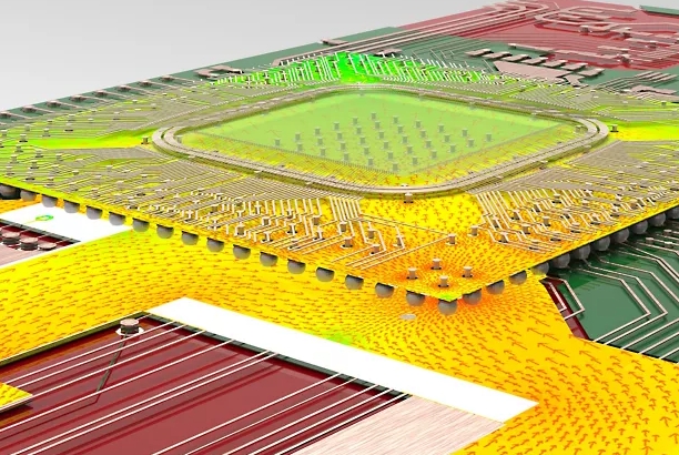
EMI Mitigation Design Considerations
When designing electronic systems with mid low loss PCBs to mitigate EMI, factors to consider are the layout of signal traces, components, and power planes. Proper layout techniques, such as minimizing trace lengths, maintaining signal integrity, and separating high-speed and low-speed signals, can help reduce signal coupling and minimize EMI emissions. Implementing a solid ground plane and using star grounding techniques to reduce ground bounce effects and prevent common-mode noise from coupling into sensitive signal traces is also necessary. Using shielded cans, conductive coatings, or grounded enclosures around sensitive components and high-frequency circuits can help contain electromagnetic radiation and prevent it from interfering with nearby circuits.
Reduce EMI using mid low loss PCB
Mid low loss PCBs can effectively reduce electromagnetic interference in electronic systems. Users can enhance signal integrity and improve system reliability by utilizing the inherent characteristics of mid low loss PCB materials and implementing effective design practices. Low- to medium-loss PCBs provide a reliable foundation in telecommunications, medical equipment, automotive electronics, or other EMI-sensitive applications.