
How to achieve low loss in high-frequency PCB?
High frequency PCB is critical in radio frequency communications and high-speed data transmission applications, which require meticulous attention to detail. Achieving low losses in high frequency PCBs is essential for engineers and designers seeking optimal performance. As a PCB manufacturer, we will tell you how to attain low-loss strategies and best practices for high-frequency PCBs.
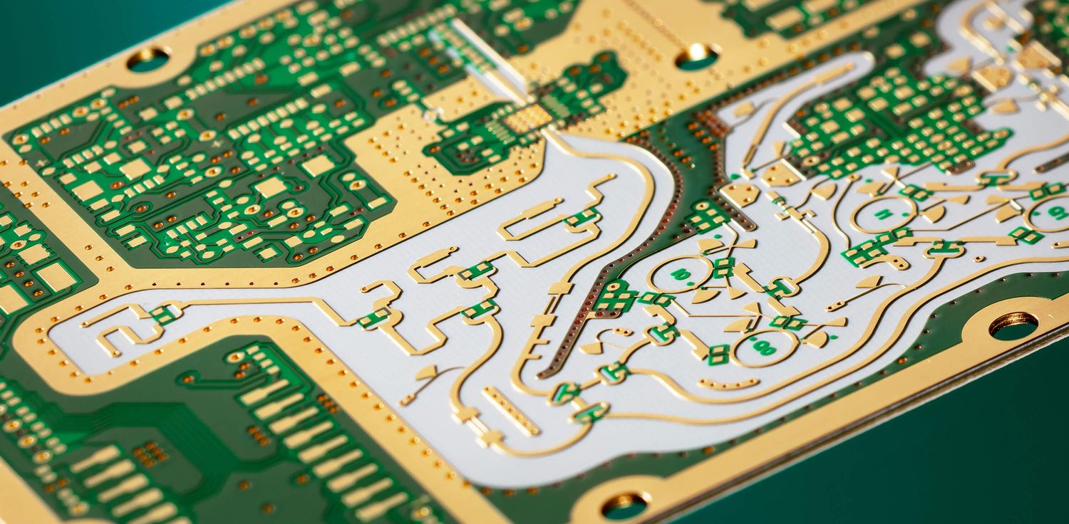
Choosing the suitable materials for high frequency PCB
Achieving low loss in high frequency PCB starts with choosing suitable materials. Choosing high-performance substrates with low dielectric constants minimizes signal loss and ensures efficient energy transfer. Materials such as PTFE (polytetrafluoroethylene) and specialized high-frequency laminates provide the necessary electrical properties to create a foundation for low-loss high-frequency PCBs. Choosing low-loss dielectric materials with low tan values is critical to maintaining signal integrity and minimizing energy dissipation.
Optimize trace and transmission line design for low-loss
Our engineers can precisely control impedance using techniques such as meticulous width adjustment, spacing considerations, and careful management of dielectric thickness. This approach minimizes signal reflections, enhances signal integrity, and reduces losses in high-frequency applications. Thoughts cause energy loss and signal distortion, and advanced simulation tools can be used to iteratively refine impedance parameters to ensure the design meets low-loss goals. Thereby enhancing the overall performance of high frequency PCB.
Effective grounding technology to achieve low loss in high frequency PCBs
Implementing a ground plane structure helps minimize ground loops and reduce electromagnetic interference. A continuous ground plane beneath the signal traces provides a low-inductance path, enhancing signal integrity and reducing losses. Incorporating ground plane stitching technology further enhances the integrity of the ground plane, reducing the potential for ground-induced losses in high frequency PCBs. In addition, effective isolation of sensitive components is also a critical step in high-frequency PCB design. Design engineers can prevent unnecessary coupling between components, minimize crosstalk, and reduce the possibility of signal loss, ensuring low-loss success through the targeted placement of isolation structures, such as isolation rings or ground isolation.
Reduce high frequency PCB losses through components
Choose low-loss components for high-frequency applications, including capacitors, inductors, and resistors. High-quality components with low equivalent series resistance (ESR) and equivalent series inductance (ESL) help achieve low losses in high frequency PCBs. Critical points in high frequency PCBs where failures can occur are at RF connectors and transmission lines. Choose connectors with low insertion loss and transmission lines with suitable impedance and attenuation characteristics. Proper termination and careful attention to transitions between different components ensure minimal damage to these critical areas. PCB engineers should consider advanced connector designs to reduce insertion loss further.
Advanced low-loss simulation and modeling technology
Utilizing electromagnetic simulation tools is extremely valuable in pursuing low losses in high frequency PCBs. These tools allow engineers to model and analyze signal behavior, helping identify potential loss areas and optimize designs accordingly. Simulation helps fine-tune parameters to ensure the final PCB design meets low-loss goals. Combining iterative design methods with prototyping can also achieve low-loss, high frequency PCBs. Prototyping allows engineers to validate designs in a real-world environment, making adjustments based on real-world observations and effectively achieving low losses for high frequency PCBs.
In the end
We have given methods and strategies to achieve low loss in high frequency PCBs. Each PCB engineer who wants to accomplish this can combine their circumstances by carefully selecting materials with good dielectric properties and implementing controlled impedance design, as mentioned above. Use effective grounding techniques, etc., to reduce losses.