
What are the design rules for a 2 layer heavy copper PCB?
The use of heavy copper in PCBs has become commonplace in industries that require high power distribution and thermal management. Specifically, 2 layer heavy copper PCB provides excellent durability for applications in automotive, power supplies, etc. However, using heavy copper creates associated problems and requires a specialized set of design rules. This blog post will tell you what design considerations we follow when designing a 2 layer heavy copper PCB.
Pay attention to copper thickness and trace width!
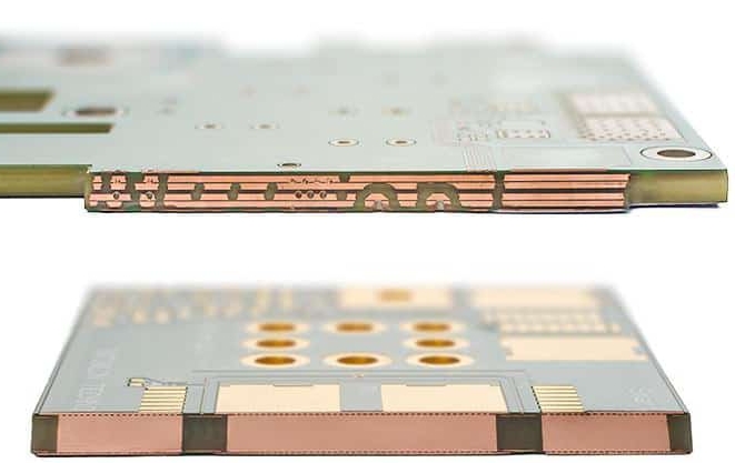
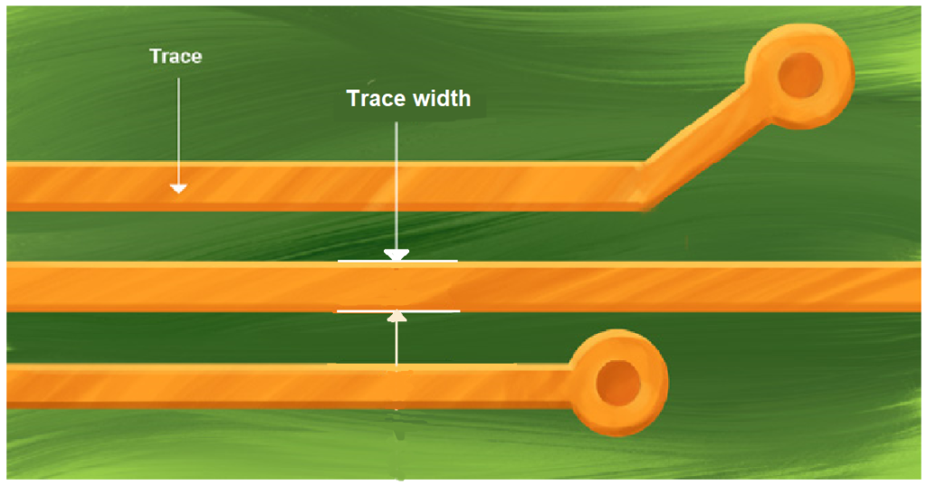
When designing a 2 layer heavy copper PCB, the copper weight per layer may be as high as 3 ounces/square foot or even 4 ounces/square foot. This increased thickness helps handle higher current loads, reduces thermal strain, and minimizes voltage drops across the circuit. With thicker copper, wider trace widths are typically required to manage the increased copper volume and ensure manufacturability. Wider traces reduce the risk of etching issues during manufacturing and reduce the trace’s resistance. As a rule, trace width should increase proportionately to copper weight. For example, a 10 oz/sq ft copper layer may require about 20-30% more trace width than a standard design.
Pay attention to thermal management when designing 2 layer heavy copper PCB
Thermal vias are standard practice for thermal management of 2-layer thick copper PCBs. This method is plated through holes that connect the top and bottom layers of the PCB and act as a channel for heat to move vertically through the board to the wider thermal surface. For better high thermal efficiency, we place thermal vias under or near heating components and arrange them in a grid pattern to maximize heat transfer. When internal heat dissipation is insufficient, we use external heat sinks, connected directly to the PCB or specific heat-generating components.

Impedance control and superposition
2 layer heavy copper PCB In PCB design, impedance control refers to maintaining a specific impedance value in the transmission line formed by the PCB traces and laminate. With a 2 layer heavy copper PCB, we use wider and thicker traces to handle the higher current, which results in lower impedance. Our designers adjust trace width, spacing, and dielectric thickness to achieve the desired impedance.
In a design, traces carrying different signals may overlap intentionally or unintentionally, causing interference if not managed properly. You can minimize crosstalk by increasing the distance between parallel traces and routing them perpendicular to each other if the crossover is unavoidable. And effectively use the ground layer to reduce the impact of signal superposition. A continuous ground plane can act as a shield between different signal layers, reducing capacitive coupling and thereby minimizing interference. We will also add decoupling capacitors near the IC power pins to reduce noise caused by signal superposition.

Design for manufacturability of 2 layer heavy copper PCB
Manufacturability is another important factor in 2 layer heavy copper PCB design, and the unique characteristics of heavy copper require adjustments to standard PCB manufacturing processes. Therefore, we consider the increased copper thickness in the design of the pads and vias to accommodate the increased ring size. Regarding material selection for the substrate, we will choose materials that can withstand the higher temperatures and pressures required to laminate thick copper layers to reduce warpage during manufacturing.
Power distribution network
We will consider these key factors when designing the power distribution network for a 2 layer heavy copper PCB. We choose a thicker copper layer to reduce resistance and improve heat dissipation to achieve a more efficient power distribution network. In a 2-layer configuration, assigning one layer primarily to the ground and another layer to power is common. This approach simplifies layout and maximizes the available area for efficient power distribution and ground planes. In the power distribution network, we will place the capacitor as close as possible to the power pin of the load component. We also use a combination of large-capacity capacitors for low-frequency stabilization and ceramic capacitors for high-frequency noise filtering.
Master the overall design
Through the specific design rules outlined in this article, you can know what we have in mind when designing a 2-layer thick copper PCB. Better know we’re guaranteed for the products you need, whether it’s a power converter, automotive system, or any application that requires efficient cooling, well-designed 2-layer thick copper PCBs are the backbone of modern electronics.