
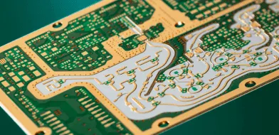
The Influence of Layer Count on Mid Low Loss PCB Signal Integrity
Low to mid low loss PCB is the backbone of most modern electronic devices, and they play a crucial role in reliable, efficient signal transmission. Different PCB layer numbers will have other impacts. In this guide, we will introduce the effect of layer number on the signal integrity of mid low loss pcbs.
Effect of Mid Low Loss PCB layers on signal integrity
The number of layers can affect the signal integrity of a Mid Low Loss PCB. As electronic devices become more compact and operate at higher frequencies, signal integrity becomes a critical consideration. One of the key factors in the effectiveness of low-loss PCBs in multilayers is the careful selection of materials and strategic placement of signal traces. High-quality dielectric materials with low loss tangent values are often used to reduce signal attenuation and maintain signal quality over longer transmission distances.
How do multiple layers improve performance?
A key aspect of multilayering is the incorporation of ground planes, which help minimize electromagnetic interference (EMI) and ensure a stable signal reference point. Layering reduces crosstalk between signals and improves the overall signal-to-noise ratio, which is critical to maintaining high-performance levels in complex electronic systems. Additionally, using advanced dielectric materials with low loss tangent values in these multilayer, low- to mid-low-loss PCBs helps reduce signal attenuation, especially at higher frequencies. This becomes imperative in applications where data rate requirements are high and maintaining signal integrity is critical.
Potential disadvantages of too many layers in Mid Low Loss PCBs
While multilayer Mid Low Loss PCBs have many advantages, we should also be aware of their potential disadvantages, especially when the number of layers is too high and the complexity of the manufacturing and assembly process increases. More layers require precise alignment and complex manufacturing techniques, resulting in higher production costs and longer lead times. This complexity also challenges quality control, potentially leading to higher defect rates.
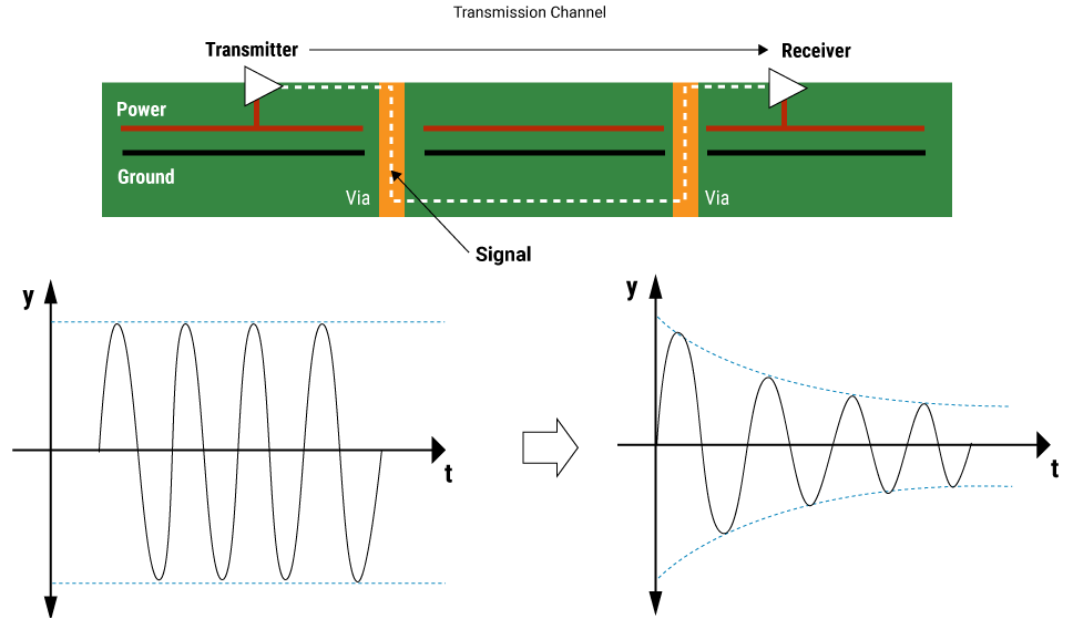
Furthermore, signal propagation delay becomes critical as the number of layers increases. Signals traveling through multiple layers may experience long delays, affecting the overall speed and responsiveness of the electronic system. Another potential issue is the increased potential for signal coupling and crosstalk between adjacent layers. Traces placed close together in multilayer PCBs can cause unintended electromagnetic interference, leading to signal integrity issues.
Customize the number of layers according to application needs
First, when customizing a Mid Low Loss PCB, it is critical to understand the application’s signal frequency and data rate. High-frequency applications may benefit from additional layers to reduce signal loss and maintain optimal signal integrity. Conversely, a lower tier count may be sufficient for less demanding applications. The power requirements of the electronic system also play a crucial role. Power planes require careful consideration to ensure efficient power distribution and minimize voltage drops. The number of layers should be adjusted to accommodate adequate power and ground planes to ensure stable operation and reduce the risk of electromagnetic interference.
The development trend of mid low loss PCB design in the future
There are several apparent trends in the development of mid low loss pcb design. One is that the continued miniaturization of electronic devices is a prominent trend. As consumer demand for smaller, more compact electronics continues to grow, there is an increasing need for low- to medium-loss PCBs that can accommodate higher functionality in limited space. High-frequency communications require low- to medium-loss PCBs with enhanced signal integrity. Future designs will likely emphasize materials and structures supporting higher data rates and frequencies, positioning low-loss PCBs as critical components in the 5G and 6G ecosystems.

At last
The impact of the number of layers on the signal integrity of low- and medium-loss PCBs is a frequently encountered problem in electronic design. By clarifying the complexity, understanding the advantages, and overcoming potential challenges, designers can design PCBs with different numbers of layers to meet different user needs. If you also want multi-layer PCBs, visit our official website to learn more!