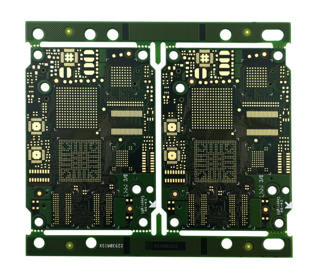
HDI PCB is a multi-layer circuit board with high wiring density, thin lines, spaces and micro-holes. They are designed to increase the functionality and performance of electronic products while reducing their size. High-Density Interconnect (HDI) PCBs represent technological advancements in printed circuit board design and manufacturing. These boards are known for their enhanced electrical performance and compact size.
Parameters and features:
Number of layers: HDI PCBs typically have more than two layers. Standard configurations include 4-layer, 6-layer, 8-layer, and up to 20 or more layers.
Microvias: Microvias are small, laser-drilled holes connecting different PCB layers, allowing for higher routing density.
Thin Lines/Spaces: HDI boards have narrow traces and gaps, usually measured in microns (μm). This allows for a more compact design.
Advanced Materials: HDI PCBs use advanced materials such as high-frequency laminates for optimal signal integrity and impedance control.
Aspect Ratio: Aspect ratio is the ratio of PCB thickness to microvia diameter. HDI boards usually have a high aspect ratio.
Blind and Buried Vias: These types of vias begin or end on inner layers, enhancing routing possibilities.
Via-in-Pad (VIP): This design places the via within the component bonding pad, allowing the use of smaller component sizes.
Manufacturing process:
Lamination: This process begins with heat and pressure to layer and bond thin core materials to create a multi-layer stack.
Drilling: Laser drilling and mechanical drilling can create micro vias and vias.
Copper Plating: After drilling, copper is deposited on the hole’s walls to create a conductive path.
Imaging: The photolithography process uses a layer of photoresist and ultraviolet light to define circuit patterns on each layer.
Etching: Chemically removing exposed copper, leaving the desired copper traces.
Copper Fill and Planarization: In the case of buried vias, any excess copper is filled and then planarized to create a flat surface.
Solder mask and screen printing: Solder mask insulates and protects copper traces, while screen printing adds component labels.
Surface Treatment: The surface of the PCB undergoes surface treatment such as ENIG (Electroless Nickel Immersion Gold) or HASL (Hot Air Solder Leveling).