
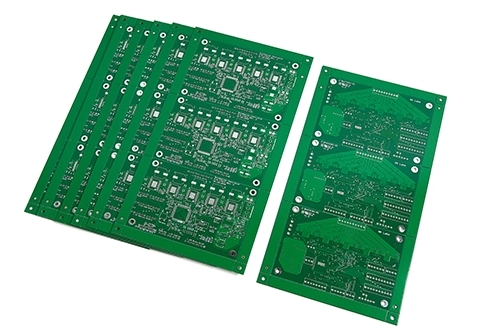
About DFM analysis of 2 layer 2OZ pcb
The role of design for manufacturability (DFM) analysis cannot be underestimated for any PCB, especially for specialized PCBs such as 2 layer 2OZ pcb. This analysis ensures that the PCB design meets manufacturability standards, thereby minimizing production issues and improving the overall reliability of the board. This comprehensive article will explore DFM analysis for 2 layer 2OZ pcbs, highlighting why it’s critical to achieving high-quality, cost-effective manufacturing results.
Key Elements of DFM Analysis of 2-Layer 2OZ PCBs
Design for Manufacturability (DFM) analysis is critical to developing 2-layer 2OZ PCBs, and comprehensive DFM analysis includes considerations for material selection, trace width, spacing, thermal management, and drilling specifications.
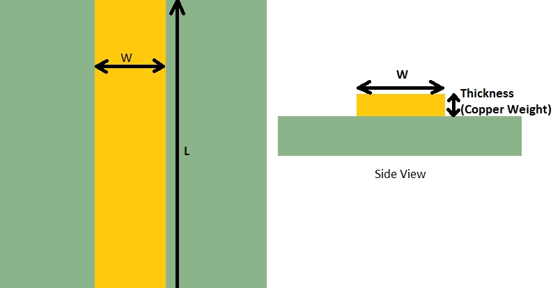
The first choice of materials for 2 layer 2OZ PCBs is typically FR-4 due to its good mechanical properties, thermal stability, and cost-effectiveness. However, since we use 2OZ copper thickness, which is thicker than standard 1OZ copper, we also need to evaluate the material handling’s ability to increase current carrying capacity and dissipate heat. Next is evaluating trace widths for 2-layer 2OZ PCBs, which typically require wider trace widths to manage the increased current capacity. DFM must evaluate minimum trace width and spacing to prevent issues such as etch defects or shorts.
DFM analysis of 2 layer 2OZ PCB also includes the evaluation of hot spots, which can be mitigated by designing appropriate copper planes that act as heat sinks. Additionally, thermal vias can be strategically placed to enhance heat transfer to external heat sinks or other layers. The drill size for a 2-layer 2OZ PCB must accommodate the hole diameter and consider the plating in the hole. DFM analysis checks and verifies whether the hole ring meets minimum specifications to reduce the risk of breakage during drilling.
Effect of Copper Weight on DFM Analysis
The main reason for choosing a heavier copper weight is to increase the current carrying capacity of 2OZ’s 2-layer PCB. This is especially important for applications that require high power density or devices that handle large electrical loads. During DFM analysis, you need to shift the focus to ensure that we scale trace widths correctly to maximize the increased capacity. Not only does heavier copper help with conductivity, but it also improves heat dissipation. In a 2 layer 2OZ PCB, the thicker copper acts as an excellent heat sink, helping to distribute and dissipate heat more efficiently throughout the board. DFM analysis must include detailed thermal modeling to identify potential hot spots and ensure the layout optimizes the thermal performance of the copper.
Available for DFM tools and software
DFM tools for 2-layer 2OZ PCBs often include advanced circuit simulation capabilities that help adjust trace widths, spacing, and layer stacking to handle increased current and thermal requirements effectively. Given the higher thermal conductivity and heat dissipation requirements of copper for 2-layer 2OZ PCBs, the DFM tool integrates thermal analysis software. This feature lets designers model how a PCB generates and dissipates heat. DFM software provides advanced algorithms for optimizing component placement, critical for space-constrained 2-layer PCBs.
Integrate DFM analysis into the PCB design process
Integrating Design for Manufacturability (DFM) analysis into the PCB design process ensures efficient manufacturing of 2 layer 2OZ PCBs and meets all performance requirements. The integration of DFM analysis begins in the initial design phase. Here, designers must consider basic DFM principles such as component placement, trace routing, and adhering to manufacturing guidelines related to board layout. For 2 layer 2OZ PCBs, it is critical to consider the increased copper thickness, which affects trace width, spacing, and pad size. It is also important to select the correct materials and layer-ups in compliance with DFM principles to ensure manufacturability and functionality. For 2 layer 2OZ PCBs, material selection also affects the board’s thermal management and mechanical strength. This integration helps make decisions that impact PCB cost and performance.
Ensure PCB manufacturing success with DFM
DFM analysis is an important step in 2-layer 2OZ PCB manufacturing, as a bridge between the design and production phases. It ensures that the board meets the required performance standards and optimizes it for associated cost-effectiveness and manufacturability. Through the DFM analysis process, manufacturers and designers can reduce the risk of rework.