
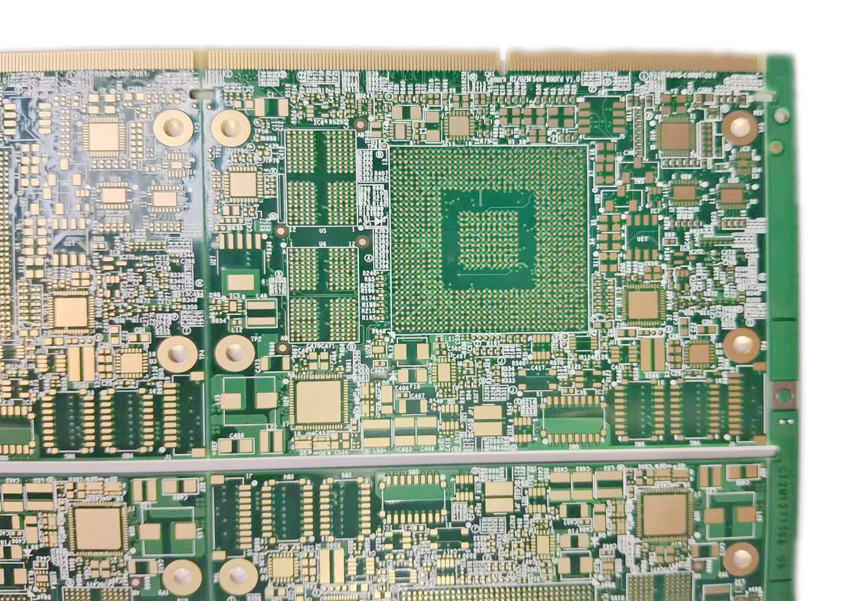
What is Via-in-Pad in HDI PCB and its Design Benefits?
In plain English, Via-in-Pad is exactly what it sounds like: you are drilling the connection hole (the via) directly into the metal landing spot (the pad) where the component gets soldered. In old-school PCB designs, the elevator (via) was in a separate hallway next to the room (pad), so you had to walk down a corridor (trace) to get there. With Via-in-Pad, the elevator door opens right inside the room. It saves a massive amount of floor space, makes the “building” (the HDI PCB) much smaller, and lets data travel much faster.
What Is Via-in-Pad Technology in High-Density Interconnect (HDI) PCB?
To really “get” via-in-pad, you have to look at the “Before vs. After” of board design. Traditionally, in standard PCBs, vias sit outside the pads, connected by a tiny wire called a “dog-bone” trace. It works, but it eats up valuable real estate and creates parasitic inductance—basically, electrical “noise” that slows things down. Via-in-pad flips the script: the hole is hidden right under the component’s foot, clearing out all that extra clutter.
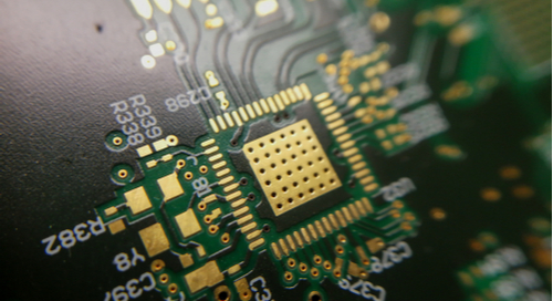
The Hardcore Engineering Part: Making this reliable is a high-precision job. First, you use a Laser Drill to create a Micro-via that is thinner than a human hair (usually 0.1mm or less). The tricky part is that you can’t leave a hole there, or the solder will get sucked down into it during assembly (a disaster called “solder wicking”). To fix this, factories use a process called POFV (Plating Over Filled Via). They plug the hole with special epoxy or copper paste, then plate a fresh layer of copper over the top and grind it down until it is perfectly flat (Planarization). If it isn’t perfectly smooth, your components won’t sit level, and the board is junk.
Compared to standard layouts, via-in-pad lets HDI PCBs reach their full potential. It allows for thinner traces and smaller holes—two things you can’t live without for high-performance boards. Whether you’re designing for a smartphone, a car’s computer, or medical gear, via-in-pad is the industry standard for keeping things small, fast, and reliable.
Key Benefits of Via-in-Pad for HDI PCB Design
Via-in-pad brings some game-changing, practical perks made for high-density electronics. It isn’t just about saving space—it fixes the main headaches of modern design by balancing size, speed, and manufacturing reliability. For designers pushing the limits, via-in-pad is usually the best move to unlock what these boards can really do.
Higher Wiring Density and Miniaturisation for HDI Boards
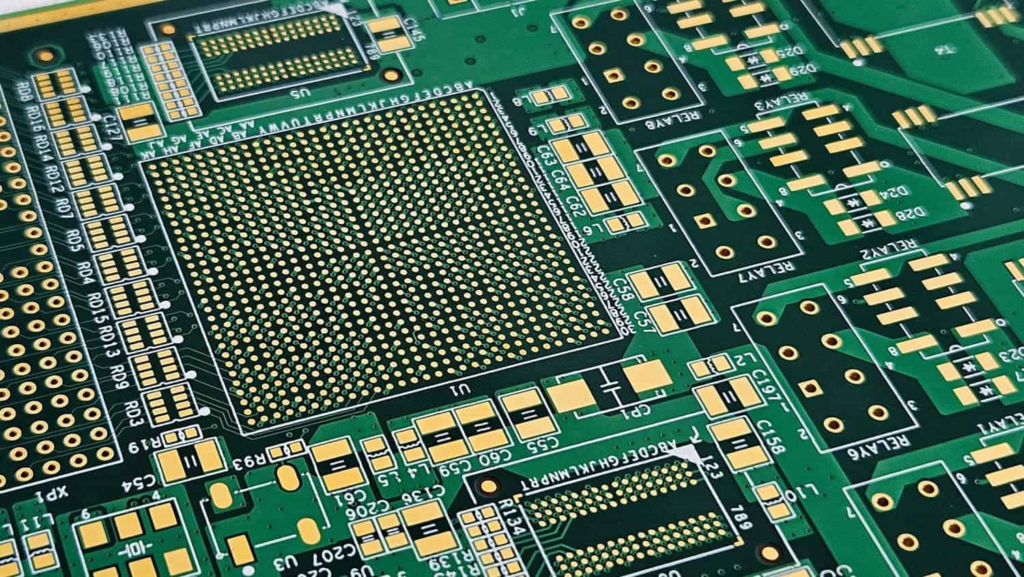
The biggest win is a huge jump in wiring density. By tucking vias under the pads, you don’t waste space on external placements. This lets you cram more components and traces into every square millimetre, making every inch count—this is the core “superpower” of HDI technology.
It also enables the use of tiny, high-pin-count packages like BGAs (Ball Grid Arrays) and QFNs with a pitch of 0.4mm or 0.5mm. These are the building blocks of modern gear that need to be small but powerful. For products like smartwatches or automotive controllers, miniaturisation is make-or-break. Honestly, a lot of today’s ultra-thin devices simply wouldn’t exist without via-in-pad.
Sharper Signal Integrity and Electrical Stability in It
Beyond saving space, via-in-pad makes the board perform better. Since the via is right under the component, the electrical path is the shortest it can possibly be. This slashes Parasitic Capacitance and Inductance, which is a big deal for keeping signal quality top-notch. It cuts down on signal delay and interference—exactly what you need for high-speed operation.
Filled vias also get rid of the risk of signal reflections and “impedance bumps”—those annoying disruptions that mess up data. When you pair this with strict Impedance Control, you get a board that keeps signals crystal clear, even in complex multilayer designs. For important gear like medical devices, this stability means a much more reliable final product.
Superior Manufacturing and Quality Control for It
A top-quality via-in-pad board is only as good as the process used to make it. It needs careful attention to detail: laser-drilling micro-vias, filling them with copper, and levelling the surface so soldering goes smoothly. These high-density boards are far more precise than standard PCBs.
Every step—from lamination to etching—is closely watched to ensure structural integrity. Quality control is strict: AOI (Automated Optical Inspection) finds surface flaws, X-rays check that the vias are filled properly (no air bubbles allowed!), and flying probe tests make sure every connection works. Before shipping, multiple manual checks ensure every board meets the high-density standards required for advanced applications.
FAQ
- What’s the difference between via-in-pad and regular vias? Via-in-pad is inside the pad to save space and boost signal quality. Regular vias sit outside and work fine for simple, low-density PCBs, but they aren’t efficient enough for high-performance HDI.
- Is via-in-pad necessary for all HDI PCB projects? Nope. It’s a must for high-density or high-speed boards. For simpler, lower-density layouts, traditional vias are more cost-effective.
- Does via-in-pad improve the reliability? Absolutely. Filled vias reduce gaps and improve electrical stability. Shorter signal paths and thorough quality control mean a longer life for the board.
- Which industries use it the most? It’s everywhere in smartphones, wearables, automotive electronics, medical devices, and high-end communication equipment.
- Does it add cost to production? Yeah, it adds a bit of cost because of the extra filling and flattening steps. But for advanced gear, the performance and space savings are totally worth the investment.
How to Optimise Your HDI PCB Design with Via-in-Pad
Getting the hang of via-in-pad tech lets you make smarter choices about layout and parts. When you use it correctly, you get higher density, clearer signals, and a much more reliable product—exactly what you need to stand out in today’s competitive market. Whether you’re designing a new product or tweaking an existing one, via-in-pad is the key to unlocking the full potential of HDI technology. Partner up with a manufacturer that specialises in precision HDI, and you’ll turn those high-end specs into a high-quality reality.