
What is gold finger PCB?
The name “gold finger pcb” sounds strange to everyone, and they don’t know what it is. They are a type of PCB. Gold finger PCBs ensure seamless connections and reliable performance in countless electronic applications. We will tell you the details of Gold finger PCB in this guide.
Understand Gold Finger PCB
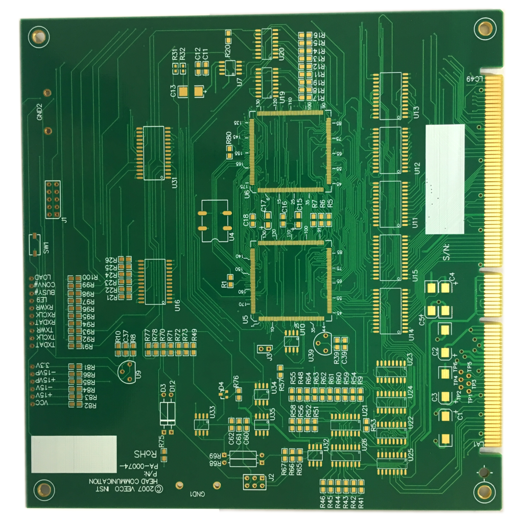
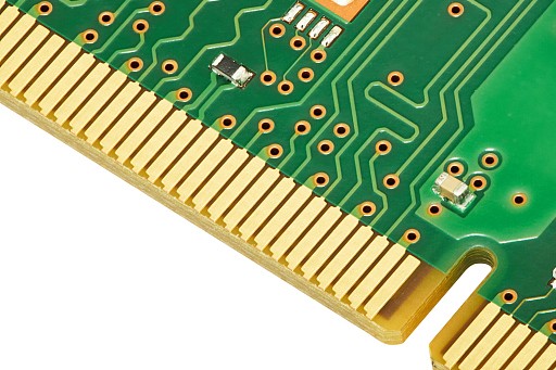
Gold finger PCB is a specialized circuit board design with gold-plated contacts common in high-performance electronic equipment. These gold-plated contacts (called “gold fingers”) serve as connectors or interfaces between the PCB and external components. Gold provides excellent electrical conductivity, corrosion resistance, and reliability, making it ideal for applications requiring high-quality connections. The gold plating on the fingers serves a dual purpose, providing excellent electrical performance while protecting against oxidation and corrosion. The properties of gold make it resistant to tarnishing, ensuring a stable and reliable connection over the long term.
Gold Finger PCB Analysis
Gold finger PCBs typically contain multiple layers of substrate material, with the number of layers depending on the complexity of the electronic device and its functional requirements. Advanced devices may feature complex multi-layer designs to accommodate higher-density components and complex circuitry. Each layer serves a specific purpose: hosting signal traces, power planes, or ground planes. Active voice: Manufacturers shape and configure the gold fingers to match corresponding connectors on other devices, ensuring a precise and secure fit. Common shapes include flat contacts, chamfered edges, and even unique shapes for proprietary connections. The arrangement and spacing of the gold fingers are customized to meet the specific requirements of the device and its intended application.
Application of gold finger PCB
Applications for “Gold Finger” PCBs span a variety of industries, enhancing performance and reliability through their unique design and gold-plated connectors.
Consumer electronics products:
Manufacturers widely use gold finger PCBs in consumer electronics, such as smartphones, tablets, and laptops. Their use ensures high-speed data transmission, power distribution, and reliable connections to various component connections.
Computing system:
High-performance computing systems, including servers and data centers, utilize Gold finger PCBs to facilitate efficient module communication. Gold-plated connectors provide a low-resistance path critical to data integrity.
Test and measuring instruments:
Precision instruments used in test and measurement applications often employ gold-finger PCBs to maintain signal accuracy and integrity. Gold-plated connectors help achieve the stable connection necessary for accurate measurements.

Quality control and testing
Gold finger PCB undergoes a meticulous gold-plating process to create gold-plated connectors. The process involves electroplating a thin layer of gold on the finger. This layer enhances electrical conductivity, corrosion resistance, and durability. Various techniques, including immersion and electroless plating, achieve precise and uniform gold coatings on connectors.
We need to ensure the integrity of Gold finger PCBs by implementing quality control measures. Active voice: The visual inspection verifies the accuracy of the gold plating, ensuring that the finger is evenly plated and defects-free. Advanced testing methods, such as automated optical inspection (AOI) and X-ray inspection, help detect any anomalies in the PCB structure, including issues with gold-plated surfaces.
What should you pay attention to when designing?
When we design a gold finger PCB, we must also carefully consider several vital factors to ensure optimal performance, reliability, and other essential aspects. We provide the precise alignment and spacing of the gold fingers to match the corresponding connector on the external device. This is crucial for a reliable connection. Also, consider the device’s form factor and external connection-specific requirements for proper gold finger placement along the edge of the PCB.
When it comes to material selection, choose a high-quality substrate material, usually fiberglass-reinforced epoxy. The next step was determining the optimal thickness of gold plating on the fingers to achieve the desired conductivity and durability. This is followed by careful inspection of routed signal traces to minimize signal distortion, crosstalk, and interference. Follow best practices for controlled impedance to ensure signal integrity. The area around the gold finger must also be reinforced to withstand mechanical stress during device insertion and removal, thereby increasing durability.
In the end
We told the details about Gold finger PCB, from its unique design and application in different industries to enhanced connectivity, durability, and other aspects. We hope that more people will know about this type of PCB through this. If you are interested in this, please visit our official website!