
Tips for designing low loss PCB in high-speed digital circuits
In high-speed digital circuits, signal integrity ensures reliable data transmission and minimizes signal attenuation. Proper low loss PCB design is critical to maintaining signal integrity and reducing losses associated with high-frequency signals. This comprehensive guide will explore essential tips and techniques for designing low loss PCBs in high-speed digital circuits, allowing engineers to achieve optimal performance and reliability.
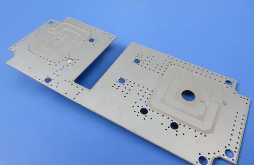
Low Loss PCB Material Selection
Low loss PCB materials are critical for designing high-speed digital circuits to ensure optimal performance and signal integrity. The choice of low loss PCB material will directly affect the electrical characteristics of the circuit, including signal speed, impedance control, and power efficiency. Traditional FR-4 materials, although widely used, can exhibit higher dielectric losses and signal distortion at higher frequencies, limiting the performance of high-speed digital circuits. Designers often choose specialized low-loss PCB materials, such as high-frequency laminates or ceramic-filled substrates. These materials have a lower dielectric constant, lower loss tangent, and higher thermal stability than FR-4, making them suitable for high-speed digital circuits.
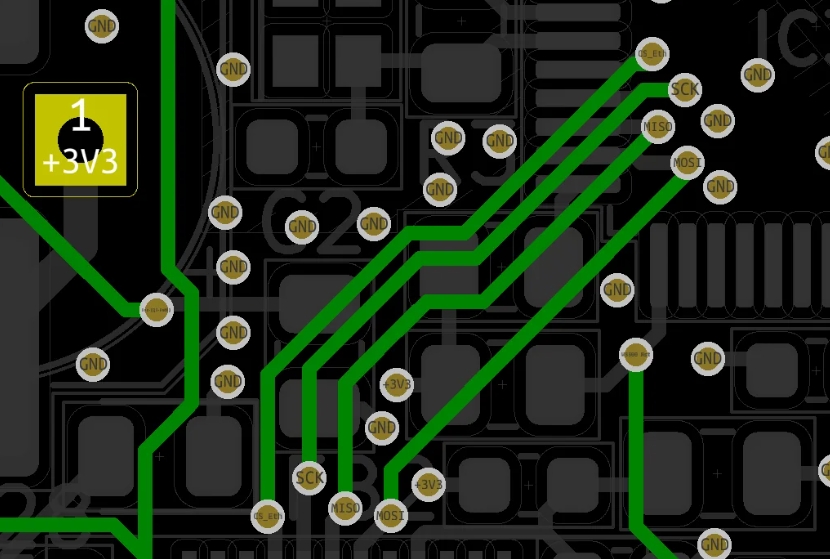
Low Loss PCB Controlled Impedance Design
Controlled impedance design is critical to ensuring the integrity of high-speed digital signals on low-loss PCBs. In high-speed digital circuits, signals travel along transmission lines in the form of electromagnetic waves. Any impedance mismatch in the transmission path can cause signal reflections, resulting in data errors, timing issues, or signal attenuation. Controlled impedance design begins with selecting PCB materials with specific dielectric properties to achieve the desired characteristic impedance. After choosing the PCB material, the designer will calculate trace width, thickness, and layer stack up to reach the target impedance value for the signal trace. Impedance control techniques such as dielectric spacing, trace width adjustment, and differential pair routing ensure consistent impedance throughout the PCB.
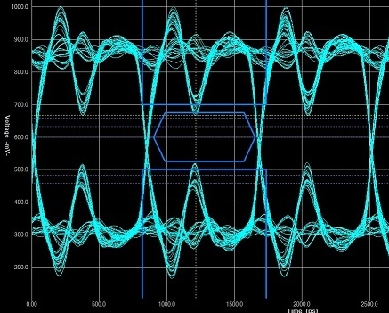
Low loss PCB signal integrity analysis
Designers use simulation tools and techniques to predict signal behavior and analyze factors that affect signal integrity. This includes accounting for signal rise times, propagation delays, and impedance mismatch along the transmission line. Impedance analysis is critical to signal integrity, especially in high-speed digital circuits. Designers calculate and verify the characteristic impedance of signal traces to ensure impedance matching and minimize signal reflections. In addition, designers can analyze signal reflections and crosstalk to identify potential sources of signal attenuation and interference. Reflections occur when a signal traveling along a transmission line encounters an impedance mismatch or discontinuity, causing signal distortion and data errors.
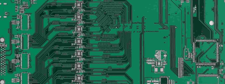
High-frequency routing technology minimizes signal distortion
A key aspect of high-frequency routing techniques is minimizing signal path lengths and optimizing trace geometries to reduce signal propagation delays and impedance variations. Shorter signal paths help minimize signal distortion and ensure faster propagation, improving overall system performance. Implement differential pair routing, matched length traces, and controlled impedance routing to mitigate signal skew and reduce signal reflections. Use proper termination techniques to improve signal integrity and minimize signal ringing. Please note signal routing guidelines and best practices to optimize high-speed signal paths.
EMI and crosstalk mitigation
Electromagnetic interference (EMI) and crosstalk can degrade signal quality and affect the performance of low-loss PCBs in high-speed digital circuits. Implement EMI shielding techniques such as ground planes, shield cans, and ferrite beads to mitigate electromagnetic interference and reduce signal noise. Use isolation techniques to minimize crosstalk between adjacent signal traces. Conduct EMI testing and analysis to identify and resolve potential sources of interference early in the design process. Additionally, designers can employ signal isolation techniques to prevent EMI propagation between different parts of the PCB. This can include physically separating sensitive components, moving signal traces away from noisy areas, or using isolation barriers to contain electromagnetic radiation.
Achieve optimal performance of high-speed digital circuits
By following the tips and techniques in this guide, engineers can optimize low loss PCB designs in high-speed digital circuits to minimize signal loss, improve signal integrity, and enhance the reliability of high-speed digital circuit applications. Through continuous design verification and testing, ensure the success of low loss PCB designs in high-speed digital circuits.