
The growing demand for Multi Layer PCB in high density data centers
High-density data centres are growing rapidly as digital transformation drives massive data processing and storage needs. From cloud computing to artificial intelligence, these facilities must support heavy workloads without downtime. To achieve this, the design of their hardware must evolve. At the core of this evolution is the Multi Layer PCB. It enables high performance, compact structure, and reliable interconnection inside complex server and networking systems. Without it, modern data centres cannot deliver the scale and speed businesses demand.
Why Data Centres Require Advanced PCB Technology
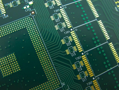
Traditional single or double-layer boards cannot handle the density of modern components. Processors, GPUs, and memory chips now require precise interconnections within limited space. Data centres also run thousands of servers simultaneously, pushing for smaller footprints and better efficiency. Multi-layer PCB designs solve these challenges by stacking multiple conductive layers on one board. This layout supports more components, reduces wiring complexity, and ensures faster data transfer. As workloads rise, such technology becomes not only useful but critical.
.jpg)
Maintaining Signal Integrity in High-Speed Systems
Data in modern data centres moves at extremely high frequencies. Any disruption can cause errors, latency, or even system failure. Signal integrity is a top concern. Multi-layer PCB technology allows the separation of power, ground, and signal layers. Designers use controlled impedance and shielding to minimise crosstalk. These measures ensure clean signal transmission even under heavy loads. For facilities running high-bandwidth applications such as streaming or real-time analytics, stable signals are essential. Without them, user experience and service reliability would collapse.
Thermal Management for Reliable Operation
Heat is a constant issue in high-density environments. Servers running around the clock generate enormous thermal loads. If heat is not managed, components fail and downtime increases. Multi-layer PCB designs help by distributing power evenly and integrating thermal vias. These vias allow heat to move away from critical components, preventing hot spots. This design improves overall durability. For data centres, where uptime translates into revenue, boards with strong thermal performance reduce maintenance costs and extend equipment life.
Space Optimisation and Compact Designs
Every rack in a data centre represents a significant investment. Operators aim to maximise performance per square foot. Multi-layer PCB supports this by reducing the need for external wiring and bulky interconnections. By integrating multiple functions into one board, systems become smaller yet more powerful. This efficiency allows more servers to fit into a limited space. As global demand for cloud services rises, compact yet capable infrastructure is a strategic advantage. Multi-layer PCB technology makes this level of optimisation achievable.
Efficient Power Distribution Across Systems
Data centres consume massive amounts of power. Stable delivery to every chip is crucial. Voltage drops or uneven supply can lead to instability. Multi-layer PCB technology addresses this through dedicated copper planes for power and ground. These planes reduce resistance, improve current flow, and ensure reliable performance. The result is not only stability but also efficiency. Lower energy waste directly impacts operating costs. For large-scale facilities, the savings from better power distribution are substantial.
Scalability for Next-Generation Applications
Emerging workloads such as AI, 5G, and edge computing demand faster and more adaptable infrastructure. Multi-layer PCB designs provide the flexibility to integrate new processors, memory modules, and interfaces without redesigning entire systems. They support higher input/output density and allow quick adaptation to industry changes. This scalability ensures that data centres can keep pace with innovation. As technologies evolve, boards that can scale effectively will determine which facilities remain competitive in the global market.
Future Outlook for Multi-layer PCB in Data Centers
The role of Multi Layer PCBs in data centres will only grow stronger. Demand for speed, density, and energy efficiency is pushing engineers to explore new materials and embedded components. Innovations such as advanced laminates and integrated cooling features will make these boards even more capable. For operators, adopting Multi Layer PCB solutions is not just a technical choice but a strategic one. They form the foundation of reliable, scalable, and cost-effective infrastructure.