
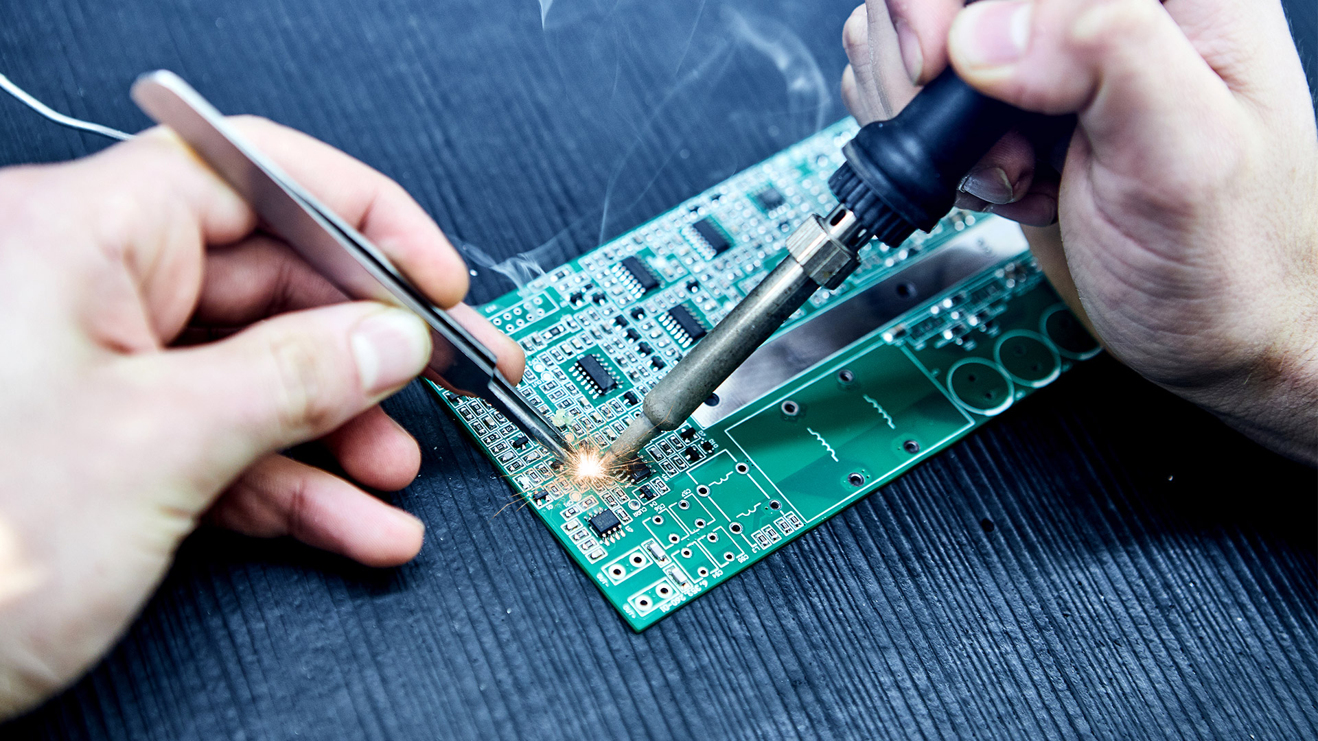
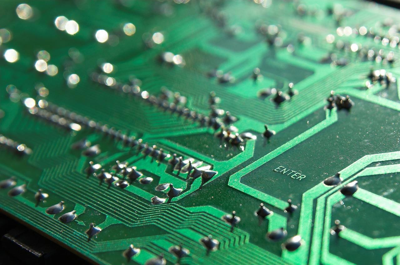
You’ve probably heard the terms “SSD circuit board” or “SSD PCB,” but what’s the real story? It’s not just a generic slab of green fibreglass; it’s a high-performance platform custom-built to be the “backbone” of your drive. In the industry, we consider it the system’s silent anchor—it’s the part that actually dictates how fast your […]
SSD PCB solutions are printed circuit boards designed specifically for solid-state storage. Their performance requirements extend beyond speed to include stability, durability, and signal integrity, and they are widely used in consumer electronics, enterprise storage, and high-performance computing. Solid-state drive PCB manufacturing focuses on long-term storage reliability, with its design, development, and production adhering to […]
SSD PCB Trends: What the Next Generation Storage Modules Hold for the SSD Market. The SSD market is expanding rapidly as data-driven technologies dominate the global economy. From hyperscale data centers to high-end gaming laptops, every device now demands faster storage. This growth has put tremendous pressure on the SSD PCB, which serves as the […]
Data center operators choose SSDs for their speed and reliability. However, the printed circuit board inside each drive — specifically, the SSD PCB — has a significant impact on both performance and reliability. Design choices on the board change thermal behaviour, signal integrity, power delivery, and testing outcomes. I explain why these choices are essential […]
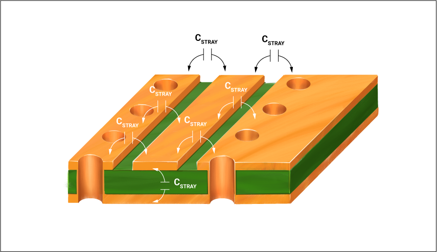
Solid-state drives (SSDs) require high-speed, reliable connections. Modern storage systems depend on stable signal paths and robust thermal performance. A poorly printed circuit board can cause data loss, latency, or failure. A multi-layer PCB architecture addresses these challenges by providing multiple conductive layers, improving signal integrity, and enhancing power distribution. Let’s explore how multi-layer designs […]
The SSD PCB plays a pivotal role in enabling the performance and efficiency of modern NVMe and PCIe drives. Unlike traditional hard drives, which rely on spinning disks and mechanical arms, SSDs use NAND flash memory mounted on PCBs to store data. This transition from mechanical to solid-state architecture hinges on the quality and layout […]
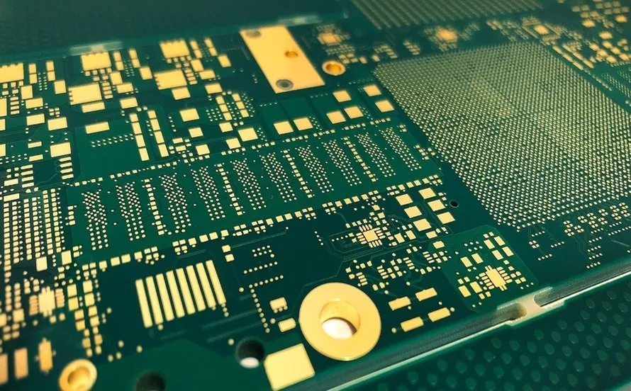
The design of an SSD PCB plays a critical role in determining both the performance and reliability of storage devices. The printed circuit board (PCB) acts as the foundation for all electronic components, including the NAND flash, controller, DRAM cache, and power management systems. Without well-engineered SSD PCBs, even the most advanced memory chips cannot […]

The base material can make or break performance when designing a reliable SSD PCB. As the demand for high-speed data storage grows, engineers and manufacturers face increasing pressure to select substrates that offer electrical stability, thermal endurance, and mechanical reliability. FR4, Polyimide, and BT Resin are the primary contenders in this arena. Each comes with […]
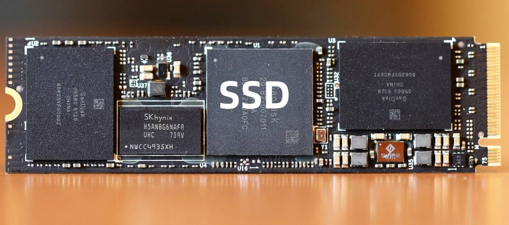
The SSD PCB is the heart of any solid-state drive, connecting all essential components that handle data storage and transmission. It houses the NAND flash memory, controller, power management ICs, DRAM (if present), and passive components that regulate the operation. Unlike mechanical drives, SSDs rely entirely on electronic components, which makes the PCB layout and […]
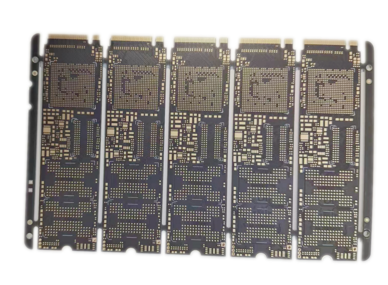
Over the past two decades, SSD PCB architecture has transformed storage technology. Starting with SATA-based designs that mimicked HDD limitations, it rapidly advanced to PCIe and NVMe interfaces that unlocked unprecedented speed and efficiency. This evolution didn’t just boost performance; it redefined how systems access data, powering everything from consumer laptops to enterprise servers. Today’s […]