
Specific Trace Design Guidelines for Heavy Copper PCB Manufacturing
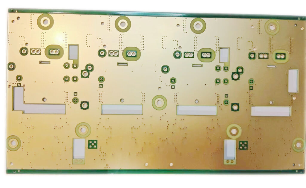
Heavy copper PCBs are a crucial solution for applications capable of high current handling, robust thermal management, and enhanced durability. We are often asked for specific trace design guidelines for Heavy Copper PCB manufacturing by many users who need to use them. If you want to know the relevant details when manufacturing heavy Copper, we will give a unified answer to these users in this guide.
Key considerations when designing traces for heavy copper PCB manufacturing
We consider several key factors when designing traces for heavy copper PCB manufacturing. First, the current carrying capacity of the trace must be regarded as. To handle a higher current than a standard PCB, wider traces are required to reduce resistance and heat generation. Another essential consideration is thermal management. Due to increased copper thickness, they are prone to heat dissipation issues, leading to uneven temperature distribution and solder joint reliability issues. Therefore, we will use a heat dissipation structure to effectively dissipate heat and maintain the optimal operating temperature of the entire circuit board. The other two points are signal integrity and mechanical stability.
Optimizing Trace Width and Thickness for Heavy Copper PCB Manufacturing
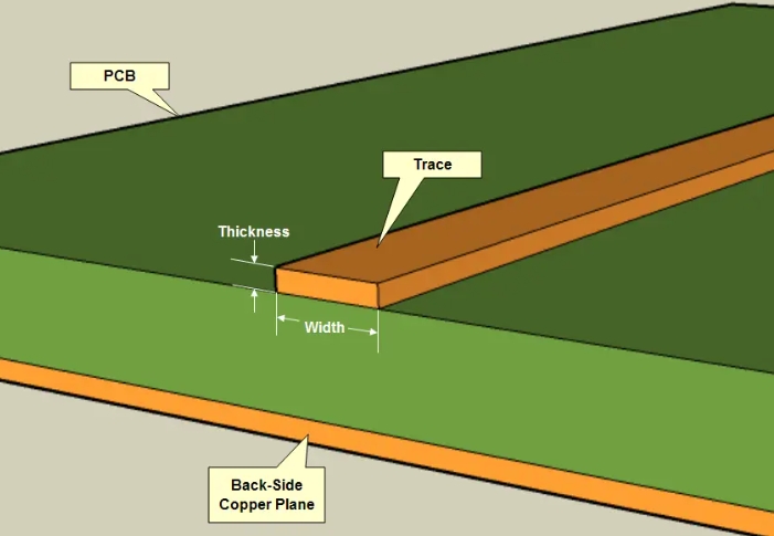
One of the factors to consider when optimizing trace widths for thick copper PCB manufacturing is determining the optimal width and thickness of the traces. Thick copper layers provide higher current-carrying capabilities and better thermal conductivity while requiring wider traces to minimize resistance and voltage drop. Therefore, our designers balance copper thickness and trace width while adhering to manufacturing capabilities and cost considerations to maximize the performance and efficiency of heavy copper PCBs.
Ensure adequate trace spacing and clearance!
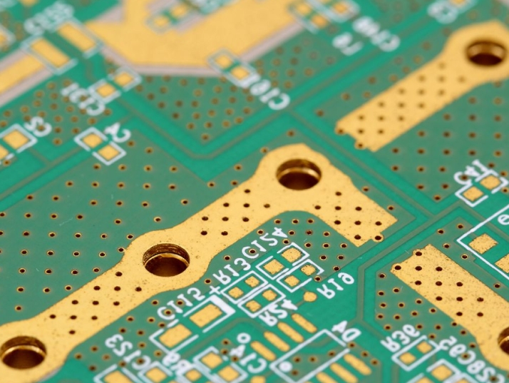
In heavy copper PCB manufacturing, we emphasize trace spacing, which is critical in mitigating the risk of arcing. Thick copper PCBs often operate at high currents, creating heat and electrical stress. Insufficient trace spacing increases the likelihood of arcing between adjacent traces, causing potential damage to the PCB and surrounding components. In addition, careful design and layout considerations allow users to maintain sufficient clearance between traces and adjacent components to mitigate the effects of electromagnetic interference and ensure signal integrity.
Implement impedance control technology!
Impedance control technology will be critical in heavy copper PCB manufacturing traces. We will first carefully select the substrate material and thickness. Controlling the thickness of the substrate allows users to fine-tune the impedance of PCB traces to meet their desired specifications. Users can achieve consistent impedance values throughout the PCB layout by carefully designing trace widths, spacing, and layer stacking. Advanced design tools and simulation technology enable users to analyze and optimize trace geometries to meet impedance requirements while minimizing signal distortion and loss.
Integrated thermal management features
One technique for integrating thermal management in heavy copper PCB manufacturing is using thermal vias, which provide a path for heat to escape from the copper layer and spread to the surrounding environment. Another critical aspect is using copper-clad areas to dissipate heat from high-power components and sensitive circuits. By strategically pouring copper around heating components, I will allow the user to minimize temperature gradients and reduce the risk of localized hot spots. We also use highly thermally conductive substrates such as aluminum backplanes or metal core PCBs to enhance heat dissipation and improve thermal performance.
Maximum performance through precision engineering
This guide lets you understand our steps when designing heavy copper PCB manufacturing traces. We will be able to ensure that the products we produce are of reliable quality. If you want to know more about the problems when manufacturing PCBs, please consult us!