
Manufacturing Process of Single Layer Aluminum PCB
With the emergence of various high-tech applications, our demand for efficient and reliable PCBs is increasing. Among the wide variety of PCB types, single layer aluminum PCB stand out due to their excellent thermal conductivity and cost-effectiveness. This guide looks at the complex manufacturing process of single-layer aluminum PCBs, allowing the designer or operator to understand the critical steps to their superior performance.
Learn about single layer aluminum PCB
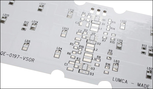
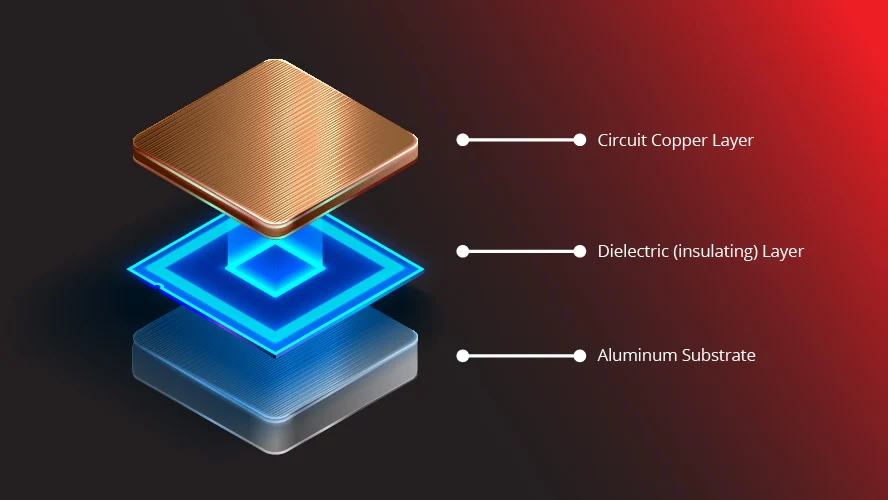
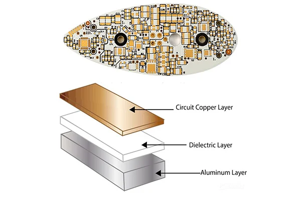
The core of a single-layer aluminum PCB is typically composed of a thermally conductive dielectric material, such as aluminum oxide (Al2O3) or polyimide, to enhance heat dissipation. A conductive layer made of aluminum is then laminated to this substrate, creating a single, compact structure. This design provides excellent thermal conductivity, making single-layer aluminum PCBs ideal for applications that require efficient heat dissipation. A significant advantage of single-layer aluminum PCBs is their simplicity, making them suitable for basic electronic circuits. Single-layer aluminum PCBs are particularly valuable in LED lighting systems, where effective thermal management is critical to maintaining optimal performance and extending the life of the LED. The aluminum layer effectively transfers heat from sensitive components, preventing overheating and ensuring reliable operation.
Raw materials and substrate preparation of single-layer aluminum PCB
The substrate, or base material, is a critical component and usually consists of a thermally conductive dielectric material. Common choices include aluminum oxide (Al2O3) or polyimide, which provide good thermal management properties. The selection of these substrates was based on their capability to effectively dissipate heat, ensuring the stability of the PCB during operation. The manufacturing process begins with the preparation of the substrate. Typically, a layer of aluminum oxide, forming the basis of the PCB, is deposited on a metal foil. Next, add the conductive layer. Manufacturers laminate thin aluminum sheets to a prepared substrate using heat and pressure.
Circuit design and etching of single layer aluminum PCB
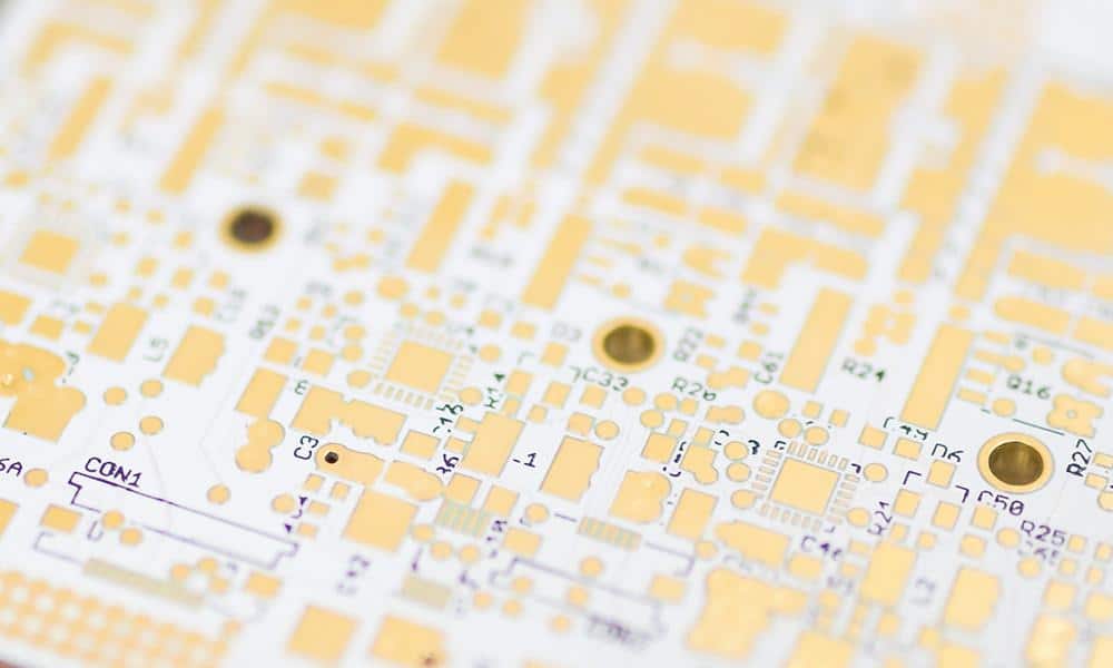
Engineers and designers use specialized software to lay out PCBs’ electrical components, traces, and connections. A single-layer aluminum PCB circuit involves selecting and placing various electronic components such as resistors, capacitors, integrated circuits, etc. Designers must carefully consider factors like signal paths, power distribution, and cooling, strategically placing traces on the aluminum layer. Proper trace layout is essential for maintaining signal integrity, minimizing interference, and optimizing electrical performance. Once the circuit design is complete, the etching process begins. This involves removing excess aluminum from the substrate to expose the desired circuit pattern. Protective material coats the aluminum layer, revealing only the design traces. Chemical etching is a standard method for selectively removing unwanted aluminum. The PCB is immersed in an etchant solution, which dissolves the unprotected aluminum.
Lamination and solder mask applications
Achieving a robust and reliable single-layer aluminum PCB involves the application of lamination and solder masks. Implementing lamination and solder mask application in a single-layer aluminum PCB begins with preparing the aluminum substrate. Surface cleaning and preparation are critical to ensure proper adhesion of subsequent layers. Deposition techniques can apply a thin copper layer to an aluminum substrate. This copper layer serves as the conductive layer for the circuit traces. A layer of dielectric material (usually composed of epoxy with reinforcement) is applied to the copper layer.
This dielectric layer provides insulation between conductive traces and serves as the foundation for the circuit. The assembled layers undergo a curing process using heat and pressure. This step ensures a strong bond between the aluminum substrate and the dielectric material, providing a solid foundation for the PCB.
Apply a layer of photoresist to the dielectric surface. Exposing a single-layer aluminum PCB to UV light through a photomask that defines the circuit pattern initiates the process. After exposure, developers remove the photoresist, revealing the desired copper pattern. Manufacturers etch away the exposed copper areas using a chemical process, leaving behind the circuit traces. Afterward, manufacturers strip the remaining photoresist, revealing the copper traces for subsequent processing.
After establishing the copper pattern, clean the PCB surface and prepare it for solder mask application. Manufacturers coat the entire single-layer aluminum PCB with a layer of solder mask, a polymer material that resists soldering and other environmental factors. This layer is essential to protect the copper traces and prevent accidental solder connections during assembly.
Quality control measures
Ensuring the quality of single layer aluminum PCBs is critical to their performance and reliability in electronic applications. Strict inspection of incoming materials, including aluminum substrate, dielectric materials, copper foil and solder mask. Material specifications, thickness and compliance with industry standards are verified.
Manufacturers take precise measurements to confirm the thickness of each layer, including the aluminum substrate, copper layers, and dielectric layers. They evaluate the bond strength between the aluminum substrate and the dielectric layer through mechanical testing.
Use automated optical inspection (AOI) or other visual inspection methods to verify the accuracy of circuit patterns to maintain the intended design. Conduct comprehensive electrical testing to evaluate the conductivity of copper traces, identify shorts, and confirm that the PCB meets electrical specifications.
In the end
We hope that by popularizing the single-layer aluminum PCB manufacturing process, more PCB operators can manufacture single-layer aluminum PCBs with more stable performance. We will continue to share knowledge about PCB. If you want to see more, please visit our official website.