
How HDI PCB Reduces Signal Interference in Complex Circuits?
In modern electronics, complex circuits demand high density, high speed, and reliable signal integrity. Using an advanced printed circuit board (PCB) architecture can greatly ease that. Among those architectures, “HDI PCB” stands out. In this post, I explain how HDI PCBe designs help cut down signal interference in complex circuits. I base the arguments on real practices and documented benefits.
Shorter Signal Paths Improve Integrity
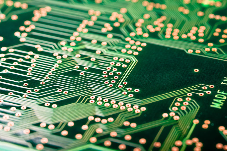
A significant advantage lies in shorter interconnect paths. In HDI boards, designers often use microvias instead of traditional through‑holes. Microvias typically have diameters of 150 microns or less (often 50–100 µm) and connect only adjacent layers. This tight, layer‑to‑layer connection dramatically reduces trace length compared to a through-hole that passes through multiple layers. Shorter paths mean fewer opportunities for signal degradation, lower latency, and minimised reflections—the result: cleaner high-speed data transmission in complex circuits.
Lower Parasitics Lead to Less Crosstalk and Noise
Standard through-hole vias and long traces bring parasitic capacitance and inductance. These parasitics cause signal coupling and crosstalk between adjacent traces — a common source of interference. HDI’s microvias, by contrast, carry much lower parasitic load due to their small size and compact geometry. This reduces mutual capacitance/inductance between nearby signals. The smaller the parasitic effects, the smaller the chance of undesired coupling. This is crucial in high‑density PCBs where many signals run side by side.
Controlled Stack‑Up and Ground/Power Plane Proximity
HDI layers often include carefully controlled stack-ups: multiple thin dielectric layers and interleaved signal, ground, and power planes. This tight layering provides signals with a well-defined return path and a stable reference (ground or power plane), which helps maintain controlled impedance. Such controlled impedance reduces signal reflections and prevents noise from propagating across the board. It also prevents ground bounce and helps contain electromagnetic interference (EMI). Many HDI manufacturers highlight that low‑loss dielectric materials and thin core layers help preserve signal integrity in high‑speed designs.
Eliminating Stub Effects and Resonances
In conventional PCBs with through-holes, vias often produce stubs or long “antenna‑like” structures. These stubs can reflect signals or even radiate unwanted electromagnetic energy at high frequencies. HDI design, using blind or buried microvias, avoids such long stubs. Because microvias connect only nearby layers and typically don’t run full board depth, the issue of signal resonance and stub-induced reflections virtually disappears. That helps maintain signal fidelity, especially in multi‑GHz applications or RF circuits.
Better EMI / RFI Performance Through Shielding and Layout Flexibility
When signal loops shrink and traces are tightly arranged with adjacent ground or power planes, the board radiates less electromagnetic interference. HDI boards support efficient EMI/RFI suppression by reducing radiation loop size and enabling via‑stitching or shielding techniques. Also, because traces run shorter and closer to the ground, near‑field coupling reduces, further reducing EMI. Many designers report that HDI reduces interference noise more noticeably than traditional designs.
High-Speed Data Circuits and RF Modules
Consider a smartphone mainboard or a 5G modem board. These PCBs often route dozens of high‑speed signals and RF paths within a small area. Using HDI microvia technology, engineers can place critical components closer, shorten trace lengths, and isolate high‑speed nets with ground planes or guard traces. In such a setup, signal attenuation, reflections, and electromagnetic leakage are significantly reduced. Several HDI board makers claim that microvia-based designs support reliable signal transmission beyond 10 Gbps while maintaining tight impedance tolerance (±5%) and a lower PDN loop inductance (under 100 pH). This leads to stable performance even under dense component layout.
Trade‑offs and Design Discipline Required
Of course, HDI isn’t magic. Achieving interference reduction depends on careful design discipline. Designers must ensure proper stack‑up, continuous reference planes, correct microvia placement, adequate spacing, and — if needed — ground stitching or guard traces between high-speed nets. They should avoid unfortunate patterns like splitting ground planes under signal traces, which can break return paths and reintroduce noise. Also, manufacturing quality matters — processes such as laser drilling, plating, filling microvias, and maintaining uniform dielectric thickness all contribute to the integrity of the final board.
Enhancing Signal Integrity in Circuits with HDI PCB
Using HDI PCB technology significantly improves signal integrity in complex circuits. By shortening signal paths, reducing parasitic effects, eliminating via stubs, and enabling controlled stack‑ups with proper grounding, HDI reduces crosstalk, EMI, and signal degradation. As electronics move toward higher speeds, tighter layouts, and more compact form factors, HDI becomes increasingly essential. For any design requiring high-speed data, RF performance, or compact multi‑function integration, adopting HDI proves a smart move. If you design or source PCBs for modern electronics, HDI offers a reliable path to cleaner signals and trustworthy performance.