
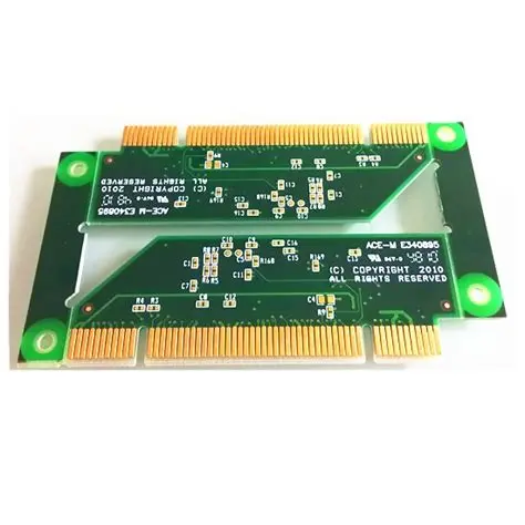
How Gold Finger PCB Edge Connectors Influence High Frequency Signal Integrity?
Printed circuit boards often rely on edge connectors for fast and reliable communication. Gold finger PCB connectors play a critical role in maintaining high-frequency signal integrity across many industries. Their design, plating quality, and geometry have a direct impact on performance, particularly in advanced computing and telecommunications.
Why Gold Plating Matters in High-Frequency Applications
Gold plating ensures low contact resistance and superior conductivity. Unlike tin or nickel finishes, gold provides a stable connection over long lifespans. At high frequencies, even minor variations in resistance can lead to losses and distortion. According to IEEE studies, gold-plated contacts minimize insertion loss, which is vital in 5G base stations and high-speed servers. Moreover, gold resists oxidation, making it ideal for demanding environments where reliability cannot be compromised. The durability of gold plating extends product lifecycles, reducing maintenance costs.
Edge Geometry and Its Role in Signal Integrity
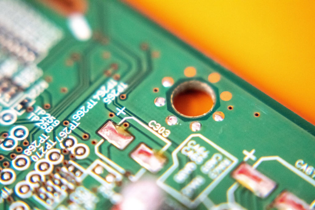
The geometry of gold finger connectors has a direct impact on impedance matching. Poorly designed edges can cause reflections, which degrade high-frequency signals. A report from Keysight Technologies highlights that mismatched impedance increases return loss, thereby reducing the adequate bandwidth. By carefully shaping connector edges and ensuring smooth transitions, engineers can preserve clean signals. The balance between plating thickness and edge shape plays a central role in high-speed designs. Therefore, precision in manufacturing gold finger PCB connectors is not just about aesthetics—it is about electrical performance.
Impact of Contact Resistance on Data Transmission
Signal distortion often comes from unstable contact resistance. With increasing data rates, any fluctuation at the connector interface can lead to jitter and packet errors. Research from Molex shows that connectors with gold plating exhibit consistent resistance values under mechanical stress. This stability ensures predictable performance in cloud servers, storage arrays, and AI systems where uninterrupted data flow is critical. Without gold finger PCB connectors, achieving this level of reliability would be extremely difficult.
Thermal Stability in High Power Applications
High-frequency systems often generate significant heat. If connectors cannot withstand temperature variations, performance quickly degrades. Gold plating enhances thermal stability, enabling connectors to maintain low resistance even at elevated temperatures. According to TE Connectivity, gold-plated contacts show better performance under thermal cycling compared to other finishes. This makes gold finger PCB connectors suitable for aerospace, automotive, radar, and 5G applications, where systems must endure extreme conditions while maintaining signal integrity.
Applications in High-speed Networking and Data Centers
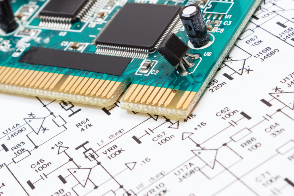
Modern data centers demand flawless performance from their hardware. Gold finger PCBs are essential in server motherboards, storage controllers, and network cards. High-frequency signals in Ethernet, InfiniBand, and PCIe systems rely on consistent performance from edge connectors. Cisco research confirms that even minor connector degradation can increase latency and reduce throughput in hyperscale networks. Using gold finger PCB connectors minimizes these risks, ensuring stable high-speed communication over extended deployment cycles.
Balancing Cost and Performance in Connector Design
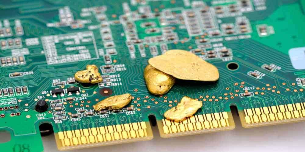
Gold is expensive, and the plating thickness must strike a balance between cost and performance. Manufacturers often optimize thickness to around 30–50 microinches, which provides durability without excessive cost. According to PCB manufacturing guidelines from Advanced Circuits, this range delivers strong wear resistance in most industrial applications. Choosing the right thickness depends on the number of insertion cycles, the expected lifespan, and the operating conditions. Engineers who select gold finger PCB connectors wisely achieve both cost efficiency and signal reliability.
Future Trends in High-Frequency PCB Design
With the growth of 5G, AI, and IoT, demand for high-frequency PCBs is accelerating. Gold finger connectors will continue to evolve with tighter tolerances and improved plating processes. Studies from Market Research Future predict steady growth in the high-speed connector market, driven by the expansion of cloud infrastructure and the increasing adoption of EV electronics. As design rules become stricter, gold finger PCB connectors will continue to be a cornerstone in ensuring high signal integrity across advanced systems.
Conclusion on Gold Finger PCB
Gold finger PCB edge connectors are more than simple contact points. They directly influence signal quality, thermal stability, and long-term reliability in high-frequency systems. By combining gold plating, precise edge geometry, and optimized thickness, engineers secure consistent performance across data centers, telecom networks, and industrial systems. For any application where signal integrity is a concern, the gold finger PCBs remain the trusted solution.