

Custom SSD PCB for High-Speed and Low-Latency Storage
Custom SSD PCB solutions drive this evolution by tailoring PCB architecture to precise performance objectives. Rather than relying on generic layouts, engineers customise each to meet specific application needs. We specialise in the research, development, and manufacturing of Custom SSD PCBs, engineering every Solution to ensure stable, high-speed, and low-latency storage tailored to real-world operating environments.
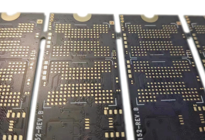
Custom SSD PCB Uses Optimised Copper Thickness and Dielectric Materials
Material selection directly shapes electrical performance in. Engineers typically select copper thickness between 1 oz and 3 oz to balance current capacity, voltage stability, and thermal performance. Thicker copper supports consistent power delivery during sustained workloads, which helps SSD controllers operate without interruption. Designers commonly pair this copper structure with FR4 or high-frequency laminated insulating copper materials, depending on signal speed requirements. By matching the copper thickness to the appropriate dielectric material, a customised SSD Circuit Board maintains signal integrity and power stability—key attributes of a reliable OEM SSD PCB Solution.
Custom SSD PCB Optimises Trace Width, Routing, and Impedance Control
High-speed data performance depends heavily on the routing strategy. In a Custom SSD PCB, engineers route high-speed signals through narrower traces to maintain precise impedance, while they reserve wider traces for power transmission to reduce resistance and heat. Beyond trace width, impedance control is critical, especially for differential pairs used in high-speed interfaces. Designers actively manage trace spacing, layer stackups, and reference planes to prevent reflection and signal loss. This routing discipline allows each OEM SSD PCB Solution to deliver accurate data transmission and predictable low latency.
Custom SSD PCB Strengthens Signal Reliability Through Via Design
Via design directly affects signal quality in high-speed storage systems. Engineers carefully control via size, placement, and copper plating quality in every step to maintain continuous signal paths across layers. Poorly designed vias introduce impedance discontinuities and electrical noise. To avoid this, Custom SSD PCB layouts use optimised via structures that preserve signal integrity and improve electrical stability. This attention to detail ensures that each OEM SSD PCB Solution performs reliably in long-term, high-speed applications.

Incorporating Thermal Management to Maintain Consistent Performance
High-speed operation generates heat, and unmanaged heat reduces performance. A well-engineered Custom SSD PCB actively addresses this challenge through structural thermal design. Engineers integrate thermal vias, heat-dissipation holes, and deep or embedded copper layers to spread heat away from controllers and memory chips. These design choices enable SSDs to maintain low latency and consistent throughput over extended operation. Effective thermal management is a defining feature of a high-quality OEM SSD PCB Solution, especially in performance-critical environments.
Choosing Surface Finishes for Reliable Assembly and Durable Performance
Surface finish selection influences assembly quality and long-term reliability. Manufacturers commonly apply ENIG, HASL, or OSP finishes in Custom SSD PCB production, depending on soldering precision and cost targets. ENIG supports fine-pitch components and stable electrical contacts, while OSP provides a cost-efficient option for controlled-assembly environments. By selecting the appropriate surface treatment, a Custom SSD PCB ensures strong solder joints and durable connections throughout its service life. This decision strengthens the overall reliability of each OEM SSD PCB Solution.
Custom SSD circuit boards ensure excellent performance through optimized layout and rigorous testing.
System performance depends on the synergistic interaction of all design elements. In custom SSD circuit boards, engineers meticulously arrange the controller, memory chips, and connectors to shorten signal paths and balance power distribution. This layout strategy minimizes latency and reduces interference. After manufacturing, the manufacturer conducts rigorous electrical testing to verify signal integrity, power delivery, and data accuracy. These tests ensure that each custom SSD circuit board meets design specifications before deployment. This verification process further elevates the performance and reliability standards of OEM (Original Equipment Manufacturer) SSD circuit board solutions.