
Thick Copper PCB vs. Rigid-Flex PCB: When to Choose Which for Complex Power Systems
A power converter can deliver hundreds of amps to a motor without overheating, warping, or failing due to vibration—the secret lies in its design: a suitable substrate, copper layer thickness, and mechanical dimensions. As a product manager at MZH Electronics, I’ve evaluated hundreds of high-current designs and guided clients in weighing the pros and cons of thick-copper PCB solutions against multilayer rigid-flex PCB structures. Therefore, I’ll guide you through practical design standards, manufacturing realities, cost considerations, and real-world application examples so you can confidently choose between thick copper PCBs and rigid-flex PCBs for your next complex power system.
Thick Copper PCB: Fundamentals and the Importance of Copper Layer Thickness for High-Current PCBs
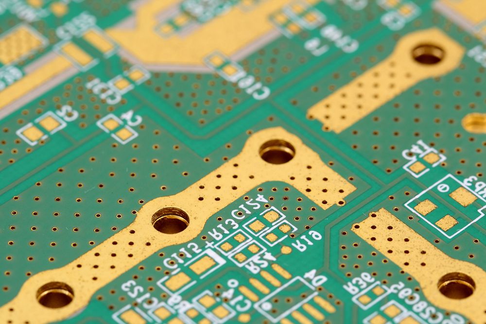
Choosing a thick copper pcb begins with understanding what “thick” means. In industry practice, copper weight is typically measured in ounces per square foot (oz/ft²) or micrometers. Standard PCBs use 1 ounce (35 micrometers) of copper. Thick copper PCBs are boards with copper layers of 3, 6, 10, or more ounces—sometimes reaching 105, 210, or even higher micrometers after plating. These thick copper layers significantly improve current-carrying capacity, reduce line resistance, and enhance thermal conductivity.
In fact, thicker copper layers can reduce I²R losses and voltage drops on power traces and buses. For example, a 6-ounce copper layer has approximately half the resistance of a 1-ounce copper layer of the same cross-section, allowing designers to achieve greater current transfer in a smaller space. Furthermore, thicker copper layers improve heat dissipation: large copper foil areas and thermal vias can transfer heat from hot spots to larger copper layers or external heatsinks. For power systems requiring sustained high current, thick copper PCB solutions typically outperform standard copper designs in both electrical and thermal performance.
Thick Copper PCB: Thermal Management Strategies and Mechanical Reliability in Power Systems
Efficient thick copper PCB designs utilize copper as both a conductor and a thermal path. MOSFETs, IGBTs, shunts, and bus connections must dissipate heat rapidly to prevent thermal runaway and ensure device lifespan. Thick copper PCB designs cleverly utilize copper foil, thermal vias, and embedded heatsinks to laterally diffuse heat and direct it to heatsinks within the chassis.
For example, a 6-ounce copper layer beneath a switching MOSFET can disperse heat over a larger area, allowing the PCB itself to act as a heatsink without the need for a bulky external heatsink. Designers should use plated-via arrays to transfer heat from top-layer components to the inner or bottom copper layers; on thick copper boards, the reliability of via plating and ring-shaped heatsinks is particularly important, as poor via filling can increase thermal resistance. Additionally, consider integrating exposed copper pads or semi-circular edges for soldering to mechanical heatsinks. These strategies can reduce junction temperature, improve switching reliability, and extend mean time between failures (MTBF). From a mechanical perspective, thick copper PCBs offer more rigidity and resistance to deformation, benefiting systems subjected to vibration or frequent thermal cycling.
Electrical Performance, Current Carrying Capacity, and Layout Best Practices
From an electrical perspective, thick copper PCBs help designers handle higher currents with lower losses and better transient response. For example, wide and solid copper layers can reduce loop inductance and equivalent series resistance (ESR), which helps handle high dI/dt conditions such as MOSFET switching and current spikes. Best practices include packing power stages tightly to minimize loop area, using wide parallel traces or continuous copper foil for the positive and negative power rails, and employing redundant vias in areas of high heat load and current demand. When designing for specific currents, use the IPC-2152 standard or a manufacturer-provided calculator to determine trace width and thickness based on temperature-rise targets. For through-holes and screw terminals, ring pads and pad sizes should be increased to withstand mechanical stress and dissipate heat. Additionally, direct-plated or soldered busbar connections to thick copper pads can further reduce connection resistance.
Manufacturing Considerations, Lead Time, and Cost Trade-offs
Using thick copper PCB technology affects manufacturing methods, yield, and cost. Thick copper boards typically require different process steps than standard 1-ounce copper boards: they may require sequential lamination, multiple plating processes, or semi-additive copper processes. Due to the longer etching or plating times, higher drilling power, and sometimes specialized tooling required for these boards, lead times and unit costs are generally increased.
Cost drivers include copper foil weight, number of layers, board area, drilling and via complexity, and surface treatments such as ENIG or HASL. Furthermore, thicker copper foil typically requires longer quality assurance cycles and more stringent process control, increasing the price per board. However, from a mass-production perspective, thicker copper-foil designs can reduce system-level costs: fewer external buses, smaller heatsinks, and lower package complexity can offset higher PCB costs. Therefore, MZH recommends conducting a total cost of ownership analysis, comparing board-level costs with system savings in weight, assembly labor, and thermal management.
Mechanical and Packaging Trade-offs for Constrained Systems
Many complex power systems face a fundamental packaging dilemma: should a mechanically continuous, thick copper board be used, or a multi-segment rigid-flex board to accommodate space constraints? Rigid-flex PCBs combine rigid sections for component placement with flexible circuitry for interconnects, folding, or dynamic movement. The contrast with thick copper boards is stark: rigid-flex boards excel in 3D packaging and vibration isolation, while thick copper boards offer significant advantages in current handling and heat dissipation.
Rigid-flex PCBs are ideal for folding circuitry into tight housings, connecting moving parts, or reducing the number of connectors that increase points of failure. They also simplify wiring-harness design and improve reliability in situations where connector fatigue is high. However, the flexible polyimide layer typically cannot carry very high continuous currents, which would otherwise result in a large copper layer that increases rigidity and complexity. While some rigid-flex PCB structures use thicker copper layers in the rigid sections, designers usually keep the copper thickness in the flexible sections moderate to maintain flexibility.
Choosing the Right PCB for Your Project
When choosing between thick copper PCBs and rigid-flex PCBs, start by asking yourself some objective questions: What are the continuous and peak current requirements? How important are thermal limitations and temperature rise? Is the design constrained by 3D packaging or motion? What are the vibration and shock characteristics? Finally, what are the costs and production limitations? Answering these questions will quickly narrow down your choices.
If continuous current, thermal performance, or low resistance are primary considerations, designers should consider thick-copper PCBs first and use hybrid rigid-flex solutions only when mechanical constraints require segmentation. Conversely, if designers need to fold the circuit board, reduce the number of connectors, or withstand repeated bending, they should prefer a rigid-flex solution and place high-current components on a rigid island with thicker copper.